
Electronics America Single-Chip Microcontrollers User's Manual

CHAPTER 13 LCD CONTROLLER/DRIVER
254
User’s Manual U15331EJ4V1UD
(1) LCD display mode register 0 (LCDM0)
LCDM0 specifies whether to enable display. It also specifies whether to enable booster circuit operation,
segment pin/common pin output, and the display mode.
LCDM0 is set with a 1-bit or 8-bit memory manipulation instruction.
RESET input sets LCDM0 to 00H.
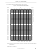
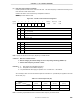
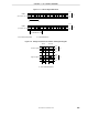
Figure 13-3. Format of LCD Display Mode Register 0
LCDON0
VAON0
0 LIPS0 0 0 0
LCDM00
LCDM0
Symbol Address After reset R/W
FFB0H 00H R/W
<7><6>5<4>3210
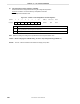
LCD controller/driver display mode selection
LCDM00
0
1
4
3
LCD display enable/disable
LCDON0
0
1
Display off (all segment outputs are deselect signal outputs)
Display on
Segment pin/common pin output control
Note
LIPS0
0
1
Booster circuit operation enable/disable
VAON0
0
1
No internal voltage boosting
Internal voltage boosting enabled
Output ground level to segment/common pin
Output select level to segment pin and LCD waveform to common pin
Number of time slices Bias mode
1/3
1/3
Note When the LCD display panel is not used, set VAON0 and LIPS0 to 0 to reduce power consumption.
Cautions 1. Bits 1 to 3 and 5 must be set to 0.
2. When operating VAON0, follow the procedure described below.
A. To stop voltage boosting after switching display status from on to off
:
1) Set to display off status by setting LCDON0 = 0.
2) Disable outputs of all the segment buffers and common buffers by setting LIPS0 = 0.
3) Stop voltage boosting by setting VAON0= 0.
B. To stop voltage boosting during display on status
:
Setting prohibited. Be sure to stop voltage boosting after setting display off.
C. To set display on from voltage boosting stop status
:
1) Start voltage boosting by setting VAON0 = 1, then wait for the voltage boost wait time
(t
VAWAIT) (refer to CHAPTER 22 ELECTRICAL SPECIFICATION).
2) Set all the segment buffers and common buffers to non-display output status by
setting LIPS0 = 1.
3) Set display on by setting LCDON0 = 1.