
Electronics America Single-Chip Microcontrollers User's Manual

CHAPTER 13 LCD CONTROLLER/DRIVER
User’s Manual U15331EJ4V1UD 257
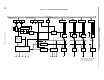
13.4 Setting LCD Controller/Driver
Set the LCD controller/driver using the following procedure.
<1> Set the LCD clock using LCD clock control register 0 (LCDC0).
<2> Set the voltage boost level using LCD voltage boost control register 0 (LCDVA0).
GAIN = 0: VLC0 = 4.5 V, VLC1 = 3 V, VLC2 = 1. 5 V
GAIN = 1: VLC0 = 3 V, VLC1 = 2 V, VLC2 = 1 V
<3> Set the time slice using LCDM00 (bit 0 of LCD display mode register 0 (LCDM0)).
<4> Enable voltage boost by setting VAON0 (bit 6 of LCDM0) (VAON0 = 1).
<5> Wait for the voltage boost wait time (t
VAWAIT) after setting VAON0 (refer to CHAPTER 22 ELECTRICAL
SPECIFICATION).
<6> Set LIPS0 (bit 4 of LCDM0) (LIPS0 = 1) and output the deselect potential.
<7> Start output corresponding to each data memory by setting LCDON0 (bit 7 of LCDM0) (LCDON0 = 1).
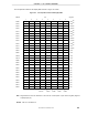
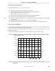
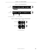
13.5 LCD Display Data Memory
The LCD display data memory is mapped at addresses FA00H to FA1BH. Data in the LCD display data memory
can be displayed on the LCD panel using the LCD controller/driver.
Figure 13-6 shows the relationship between the contents of the LCD display data memory and the
segment/common outputs.
That part of the display data memory which is not used for display can be used as ordinary RAM.
Figure 13-6. Relationship Between LCD Display Data Memory Contents and Segment/Common Outputs
(When Using S16 to S27)
S27FA1BH
S26FA1AH
S25FA19H
FA18H
S24
S2FA02H
S1FA01H
S0FA00H
COM3 COM2 COM1 COM0
b
7
b
6
b
5
b
4
b
3
b
2
b
1
b
0
Address
Caution No memory has been installed as the higher 4 bits of the LCD display data memory. Be sure to
set them to 0.