
Electronics America Single-Chip Microcontrollers User's Manual

CHAPTER 13 LCD CONTROLLER/DRIVER
266
User’s Manual U15331EJ4V1UD
13.8 Supplying LCD Drive Voltages VLC0, VLC1, and VLC2
The
µ
PD789489 Subseries contains a booster circuit (×3 only) to generate a supply voltage to drive the LCD. The
internal LCD reference voltage is output from the V
LC2 pin. A voltage two times higher than that on VLC2 is output from
the V
LC1 pin and a voltage three times higher than that on VLC2 is output from the VLC0 pin.
The LCD reference voltage (V
LC2) can be specified by setting LCD boost control register 0 (LCDVA0).
The
µ
PD789489 Subseries requires an external capacitor (recommended value: 0.47
µ
F) because it employs a
capacitance division method to generate a supply voltage to drive the LCD.
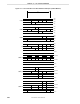
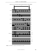
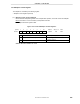
Table 13-7. Output Voltages of V
LC0 to VLC2 Pins
LCDVA0 GAIN = 0 GAIN = 1
LCD drive power supply pin
VLC0 4.5 V 3.0 V
VLC1 3.0 V 2.0 V
VLC2 (LCD reference voltage) 1.5 V 1.0 V
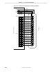
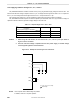
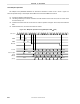
Cautions 1. When using the LCD function, do not leave the V
LC0, VLC1, and VLC2 pins open. Refer to
Figure 13-15 for connection.
2. Since the LCD drive voltage is separate from the main power supply, a constant voltage
can be supplied regardless of V
DD fluctuation.
Figure 13-15. Example of Connecting Pins for LCD Driver
V
LC0
V
LC1
V
LC2
C2 C3 C4
CAPH
C1
External pin
C1 = C2 = C3 = C4 = 0.47 F
CAPL
µ
Remark Use a capacitor with as little leakage as possible.
In addition, make C1 a nonpolar capacitor.