
Electronics America Single-Chip Microcontrollers User's Manual

CHAPTER 1 GENERAL
30 User’s Manual U15331EJ4V1UD
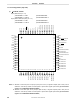
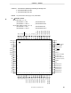
Notes 1. Whether to use these pins as input port pins (P70 to P73) or segment outputs (S16 to S19) can be
selected in 1-bit units by means of a mask option or port function register (refer to 4.3 (3) Port function
registers and CHAPTER 20 MASK OPTIONS).
2. Whether to use these pins as I/O port pins (P80 to P87) or segment outputs (S20 to S27) can be
selected in 1-bit units by means of a mask option or port function register (refer to 4.3 (3) Port function
registers and CHAPTER 20 MASK OPTIONS).
Cautions 1. Connect the IC (Internally Connected) pin directly to V
SS.
2. Connect the AV
DD pin to VDD.
3. Connect the AV
SS pin to VSS.
Remark The parenthesized values apply to the
µ
PD78F9489.
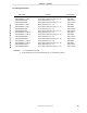
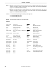
Pin Name
ANI0 to ANI7: Analog input
ASCK20: Asynchronous serial input
AV
DD: Analog power supply
AV
SS: Analog ground
CAPH, CAPL: LCD power supply capacitance
control
COM0 to COM3: Common output
CPT20: Capture trigger input
IC0: Internally connected
INTP0 to INTP3: External interrupt input
KR0 to KR7: Key return
KR00 to KR07: Key return
KR10 to KR17: Key return
P00 to P07: Port 0
P10, P11: Port 1
P20 to P25: Port 2
P30 to P34: Port 3
P60 to P67: Port 6
P70 to P73: Port 7
P80 to P87: Port 8
RESET: Reset
RIN: Remote control input
RxD0: Receive data
S0 to S27: Segment output
SCK10: Serial clock input/output
SI10: Serial data input
SO10: Serial data output
SCK20: Serial block input/output
SI20: Serial data input
SO20: Serial data output
TMI60, 61: Timer input
TO20,50,60,61: Timer output
TxD0: Transmit data
V
DD: Power supply
V
LC0 to VLC2: Power supply for LCD
V
PP: Programming power supply
V
SS: Ground
X1, X2: Crystal (Main system clock)
XT1, XT2: Crystal (Subsystem clock)