
Electronics America Single-Chip Microcontrollers User's Manual


CHAPTER 19 FLASH MEMORY VERSION
324 User’s Manual U15331EJ4V1UD
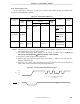
19.1.3 On-board pin processing
When performing programming on the target system, provide a connector on the target system to connect the
dedicated flash programmer.
An on-board function that allows switching between normal operation mode and flash memory programming mode
may be required in some cases.
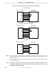
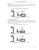
<V
PP pin>
In normal operation mode, input 0 V to the V
PP pin. In flash memory programming mode, a write voltage of 10.0 V
(TYP.) is supplied to the V
PP pin, so perform either of the following.
(1) Connect a pull-down resistor (RV
PP = 10 kΩ) to the VPP pin.
(2) Use the jumper on the board to switch the V
PP pin input to either the programmer or directly to GND.
A V
PP pin connection example is shown below.
Figure 19-4. VPP Pin Connection Example
PD78F9488,
PD78F9489
V
PP
Connection pin of dedicated flash programmer
Pull-down resistor (RV
PP
)
µ
µ
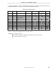
<Serial interface pin>
The following shows the pins used by the serial interface.
Serial Interface Pins Used
3-wire serial I/O SI20, SO20, SCK20
3-wire serial I/O with handshake SI20, SO20, SCK20, P11 (HS)
UART RxD20, TxD20
When connecting the dedicated flash programmer to a serial interface pin that is connected to another device on-
board, signal conflict or abnormal operation of the other device may occur. Care must therefore be taken with such
connections.