
Electronics America Single-Chip Microcontrollers User's Manual


342 User’s Manual U15331EJ4V1UD
CHAPTER 22 ELECTRICAL SPECIFICATIONS (
µ
PD789488, 78F9488, 789489, 78F9489)
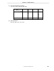
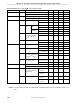
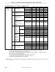
Absolute Maximum Ratings (TA = 25°C)
Parameter Symbol Conditions Ratings Unit
VDD Power supply voltage
AV
DD
V
DD = AVDD −0.3 to +6.5 V
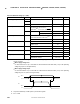
VPP
µ
PD78F9488, 78F9489 only, Note 1 −0.3 to +10.5 V
VI1 P00 to P07, P10, P11, P20 to P25, P30 to
P34, P60 to P67, P70 to P73
Note 2
,
P80 to P87
Note 2
, X1, X2, XT1, XT2, RESET
−0.3 to V
DD + 0.3
Note 3
V
N-ch open drain −0.3 to +13 V
Input voltage
V
I2 P50 to P53
On-chip pull-up resistor −0.3 to V
DD + 0.3
Note 3
V
P00 to P07, P10, P11, P20 to P25,
P30 to P34, P50 to P53, P80 to P87
Note 2
−0.3 to V
DD + 0.3
Note 3
V Output voltage VO
S0 to S15, S16 to S27
Note 2
, COM0 to COM3 −0.3 to VLC0 + 0.3 V
Per pin −10 mA Output current, high IOH
Total for all pins −30 mA
Per pin 30 mA Output current, low IOL
Total for all pins 160 mA
Operating ambient temperature TA Normal operation −40 to +85 °C
Flash memory programming 10 to 40 °C
Storage temperature Tstg
µ
PD789488, 789489 −65 to +150 °C
µ
PD78F9488, 78F9489 −40 to +125 °C
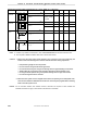
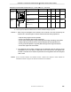
Notes 1. Make sure that the following conditions of the VPP voltage application timing are satisfied when the flash
memory is written.
• When supply voltage rises
V
PP must exceed VDD 10
µ
s or more after VDD has reached the lower-limit value (1.8 V) of the operating
voltage range (see a in the figure below).
• When supply voltage drops
VDD must be lowered 10
µ
s or more after VPP falls below the lower-limit value (1.8 V) of the operating
voltage range of V
DD (see b in the figure below).
1.8 V
V
DD
0 V
0 V
V
PP
1.8 V
a b
2. Only when selected by a mask option or port function register
3. 6.5 V or less