
Electronics America Single-Chip Microcontrollers User's Manual


CHAPTER 22 ELECTRICAL SPECIFICATIONS (
µ
PD789488, 78F9488, 789489, 78F9489)
User’s Manual U15331EJ4V1UD 345
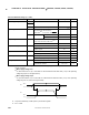
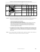
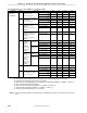
Subsystem Clock Oscillator Characteristics (TA = –40 to +85°C, VDD = 1.8 to 5.5 V)
Resonator Recommended Circuit Parameter Conditions MIN. TYP. MAX. Unit
Oscillation frequency
(f
XT)
Note 1
32 32.768 35 kHz
VDD = 4.5 to 5.5 V 1.2 2
Crystal
resonator
XT2XT1
(V
SS
)
C4
C3
R1
Oscillation stabilization
time
Note 2
V
DD = 1.8 to 5.5 V 10
s
XT1 input frequency
(f
XT)
Note 1
32 35 kHz
External
clock
XT1
XT2
XT1 input high-/low-level
width (t
XTH, tXTL)
14.3 15.6
µ
s
Notes 1. Indicates only oscillator characteristics. Refer to AC Characteristics for instruction execution time.
2. Time required to stabilize oscillation after V
DD reaches oscillation voltage range MIN.
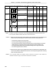
Cautions 1. When using the subsystem clock oscillator, wire as follows in the area enclosed by the
broken lines in the above figure to avoid an adverse effect from wiring capacitance.
• Keep the wiring length as short as possible.
• Do not cross the wiring with the other signal lines.
• Do not route the wiring near a signal line through which a high fluctuating current flows.
• Always make the ground point of the oscillator capacitor the same potential as V
SS.
• Do not ground the capacitor to a ground pattern through which a high current flows.
• Do not fetch signals from the oscillator.
2. The subsystem clock oscillator is designed as a low-amplitude circuit for reducing current
consumption, and is more prone to malfunction due to noise than the main system clock
oscillator. Particular care is therefore required with the wiring method when the subsystem
clock is used.
Remark For the resonator selection and oscillator constant, customers are required to either evaluate the
oscillation themselves or apply to the resonator manufacturer for evaluation.