
Electronics America Single-Chip Microcontrollers User's Manual


CHAPTER 22 ELECTRICAL SPECIFICATIONS (
µ
PD789488, 78F9488, 789489, 78F9489)
350 User’s Manual U15331EJ4V1UD
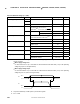
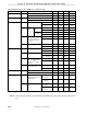
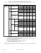
DC Characteristics (TA = –40 to +85°C, VDD = 1.8 to 5.5 V) (5/6)
Parameter Symbol Conditions MIN. TYP. MAX. Unit
VDD = 5.0 V ±10%
Note 2
2.5 5.0 mA
VDD = 3.0 V ±10%
Note 3
0.5 1.2 mA
IDD1 5.0 MHz crystal oscillation
operation mode
(C1 = C2 = 22 pF)
V
DD = 2.0 V ±10%
Note 3
0.3 0.6 mA
VDD = 5.0 V ±10%
Note 2
1.0 2.0 mA
VDD = 3.0 V ±10%
Note 3
0.35 0.8 mA
IDD2 5.0 MHz crystal oscillation
HALT mode
Note 4
(C1 = C2 = 22 pF)
V
DD = 2.0 V ±10%
Note 3
0.1 0.4 mA
VDD = 5.0 V ±10% 38 100
µ
A
VDD = 3.0 V ±10% 13 50
µ
A
32.768 kHz crystal
oscillation operation
mode
Note 5
(C3 = C4 = 22 pF, R1 =
220kΩ)
V
DD = 2.0 V ±10% 7 25
µ
A
VDD = 5.0 V ±10% 150 250
µ
A
IDD3
32.768 kHz crystal
oscillation operation × 4
multiplication operation
mode
Note 5
(C3 = C4 = 22 pF, R1 =
220kΩ)
V
DD = 3.0 V ±10% 75 160
µ
A
VDD = 5.0 V ±10% 25 70
µ
A
VDD = 3.0 V ±10% 8 32
µ
A
LCD not
operating
Note 4
V
DD = 2.0 V ±10% 5 15
µ
A
VDD = 5.0 V ±10% 28 79
µ
A
VDD = 3.0 V ±10% 10 40
µ
A
32.768 kHz
crystal
oscillation
HALT
mode
Note 5
(C3 = C4 =
22 pF, R1 =
220kΩ)
LCD
operating
Note 7
V
DD = 2.0 V ±10% 7 27
µ
A
VDD = 5.0 V ±10% 25 70
µ
A LCD not
operating
Note 4
V
DD = 3.0 V ±10% 8 32
µ
A
VDD = 5.0 V ±10% 28 79
µ
A
IDD4
32.768 kHz
crystal
oscillation × 4
multiplication
HALT
mode
Note 5
(C3 = C4 =
22 pF, R1 =
220kΩ)
LCD
operating
Note 7
V
DD = 3.0 V ±10% 10 40
µ
A
VDD = 5.0 V ±10% 0.1 10
µ
A
VDD = 3.0 V ±10% 0.05 5
µ
A
IDD5 STOP mode
Note 6
V
DD = 2.0 V ±10% 0.05 3
µ
A
VDD = 5.0 V ±10%
Note 2
5.0 6.7 mA
VDD = 3.0 V ±10%
Note 3
1.5 2.2 mA
Power supply
current
Note 1
(
µ
PD789489)
I
DD6 5.0 MHz crystal oscillation
A/D operating mode
Note 8
(C1 = C2 = 22 pF)
V
DD = 2.0 V ±10%
Note 3
0.8 1.6 mA
Notes 1. The port current (including the current that flows to on-chip pull-up resistors) is not included.
2. High-speed mode operation (when the processor clock control register (PCC) is set to 00H)
3. Low-speed mode operation (when PCC is set to 02H)
4. When the LCD is not operating and the booster circuit is operating (LCDON0 = 0, VAON0 = 1, LIPS0 = 1).
5. When the main system clock is stopped
6. When the LCD is not operating (LCDON0 = 0, VAON0 = 0, LIPS0 = 0)
7. Then the LCD is operating (LCDON0 = 1, VAON0 = 1, LIPS0 = 1)
8. This is the total current that flows to V
DD and AVDD.
Remark Unless otherwise specified, the characteristics of alternate-function pins are the same as those of port
pins.