
Electronics America Single-Chip Microcontrollers User's Manual

CHAPTER 22 ELECTRICAL SPECIFICATIONS (
µ
PD789488, 78F9488, 789489, 78F9489)
User’s Manual U15331EJ4V1UD 355
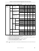
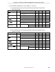
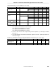
(3) Serial interface 1A0 (SIO1A0) (TA = –40 to +85°C, VDD = 1.8 to 5.5 V)
(a) 3-wire serial I/O mode, 3-wire serial I/O mode with automatic transmit/receive function
(internal clock output)
Parameter Symbol Conditions MIN. TYP. MAX. Unit
VDD = 2.7 to 5.5 V 800 ns SCK10 cycle time tKCY4
V
DD = 1.8 to 5.5 V 3200 ns
VDD = 2.7 to 5.5 V tKCY4/2–50 ns SCK10 high-/low-level
width
tKH4,
t
KL4
V
DD = 1.8 to 5.5 V tKCY4/2–150 ns
VDD = 2.7 to 5.5 V 150 ns SI10 setup time
(to SCK10↑)
tSIK4
V
DD = 1.8 to 5.5 V 500 ns
VDD = 2.7 to 5.5 V 400 ns SI10 hold time
(from SCK10↑)
tKSI4
V
DD = 1.8 to 5.5 V 600 ns
VDD = 2.7 to 5.5 V 0 250 ns Delay time from SCK10↓
to SO10 output
tKSO4 R = 1 kΩ, C = 100 pF
Note
V
DD = 1.8 to 5.5 V 0 1000 ns
Note R and C are the load resistance and load capacitance of the SO10 output line.
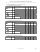
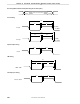
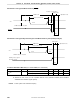
(b) 3-wire serial I/O mode, 3-wire serial I/O mode with automatic transmit/receive function
(external clock input)
Parameter Symbol Conditions MIN. TYP. MAX. Unit
VDD = 2.7 to 5.5 V 800 ns SCK10 cycle time tKCY5
V
DD = 1.8 to 5.5 V 3200 ns
VDD = 2.7 to 5.5 V 400 ns SCK10 high-/low-level
width
tKH5,
t
KL5
V
DD = 1.8 to 5.5 V 1600 ns
VDD = 2.7 to 5.5 V 100 ns SI10 setup time
(to SCK10↑)
tSIK5
V
DD = 1.8 to 5.5 V 150 ns
VDD = 2.7 to 5.5 V 400 ns SI10 hold time
(from SCK10↑)
tKSI5
V
DD = 1.8 to 5.5 V 600 ns
VDD = 2.7 to 5.5 V 0 300 ns Delay time from SCK10↓
to SO10 output
tKSO5 R = 1 kΩ, C = 100 pF
Note
V
DD = 1.8 to 5.5 V 0 1000 ns
Note R and C are the load resistance and load capacitance of the SO10 output line.