
Electronics America Single-Chip Microcontrollers User's Manual

CHAPTER 22 ELECTRICAL SPECIFICATIONS (
µ
PD789488, 78F9488, 789489, 78F9489)
User’s Manual U15331EJ4V1UD 359
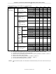
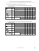
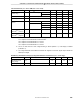
LCD Characteristics (TA = –40 to +85°C, VDD = 1.8 to 5.5 V)
Parameter Symbol Conditions MIN. TYP. MAX. Unit
GAIN = 1 0.84 1.0 1.165 V LCD output voltage
variation range
VLCD2 C1 to C4
Note 1
= 0.47
µ
F
GAIN = 0 1.26 1.5 1.74 V
Doubler output VLCD1 C1 to C4
Note 1
= 0.47
µ
F 2VLCD2 –0.1 2VLCD2 2VLCD2 V
Tripler output VLCD0 C1 to C4
Note 1
= 0.47
µ
F 3VLCD2 –0.15 3VLCD2 3VLCD2 V
GAIN = 0 1.8 ≤ VDD < 5.5 V 0.5 s
5.0 ≤ VDD ≤ 5.5 V 2.0 s
4.5 ≤ VDD < 5.0 V 1.0 s
Voltage boost wait
time
Note 2
t
VAWAIT
GAIN = 1
1.8 ≤ V
DD < 4.5 V 0.5 s
LCD output voltage
differential
Note 3
(common)
V
ODC IO = ±5
µ
A 0 ±0.2 V
LCD output voltage
differential
Note 3
(segment)
V
ODS IO = ±1
µ
A 0 ±0.2 V
Notes 1. This is a capacitor that is connected between voltage pins used to drive the LCD.
C1: A capacitor connected between CAPH and CAPL
C2: A capacitor connected between V
LC0 and VSS
C3: A capacitor connected between V
LC1 and VSS
C4: A capacitor connected between V
LC2 and VSS
2. This is the wait time from when voltage boosting is started (VAON0 = 1) until display is enabled
(LCDON0 = 1).
3. The voltage differential is the difference between the segment and common signal output’s actual and
ideal output voltages.
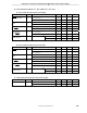
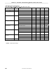
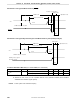
Data Memory STOP Mode Low Supply Voltage Data Retention Characteristics (T
A = –40 to +85°C)
Parameter Symbol Conditions MIN. TYP. MAX. Unit
Data retention power
supply voltage
VDDDR 1.8 5.5 V
Release signal set time tSREL 0
µ
s