
Electronics America Single-Chip Microcontrollers User's Manual

CHAPTER 2 PIN FUNCTIONS
User’s Manual U15331EJ4V1UD
45
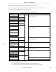
2.3 Pin I/O Circuits and Recommended Connection of Unused Pins
The I/O circuit type of each pin and recommended connection of unused pins are shown in Table 2-1.
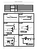
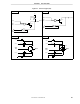
For the I/O circuit configuration of each type, see Figure 2-1.
Table 2-1. Types of Pin I/O Circuits (1/2)
Pin Name I/O Circuit Type I/O Recommended Connection of Unused Pins
P00/KR0 to P07/KR7
Note 1
P00/KR00 to P07/KR07
Note 2
8-A
P10, P11 5-A
P20/SCK20/ASCK20 8-A
P21/SO20/TxD20 5-A
P22/SI20/RxD20
P23/SCK10
8-A
P24/SO10 5-A
P25/SI10
Input: Independently connect to V
DD or VSS via a resistor.
Output: Leave open.
P30/INTP0/TO50/
TMI60
P31/INTP1/TO60
P32/INTP2/TO61/
TMI61
P33/INTP3/CPT20/
TO20
P34
Note 1
P34/RIN
Note 2
8-A
Input: Independently connect to V
SS via a resistor.
Output: Leave open.
P50 to P53
(mask ROM version)
13-W
P50 to P53
(flash memory version)
13-V
I/O
Input: Independently connect to V
DD via a resistor.
Output: Leave open.
P60/ANI0 to P67/ANI7
Note 1
P60/ANI0/KR10 to
P67/ANI7/KR17
Note 2
9-C
P70 to P73
Note 3
2-H
Input Connect to V
DD or VSS.
P80 to P87
Note 3
5-K I/O Input: Independently connect to VDD or VSS via a resistor.
Output: Leave open.
COM0 to COM3 18
S0 to S15
S16 to S19
Note 4
S20 to S27
Note 4
17
Output
CAPH, CAPL
VLC0 to VLC2
Leave open.
AVDD Connect directly to VDD
AVSS
– –
Connect directly to VSS
Notes 1. When
µ
PD789488, 78F9488 is used.
2. When
µ
PD789489, 78F9489 is used.
3. Only when port pin is selected by mask option or port function register.
4. Only when segment output pin is selected by mask option or port function register.