DATA SHEET MOS INTEGRATED CIRCUIT µPD75P3116 4-BIT SINGLE-CHIP MICROCONTROLLER The µPD75P3116 replaces the µPD753108’s internal mask ROM with a one-time PROM, and features expanded ROM capacity. Because the µPD75P3116 supports programming by users, it is suitable for use in evaluation of systems in the development stage using the µPD753104, 753106, or 753108, and for use in small-scale production. Detailed information about functions is provided in the following User’s Manual.
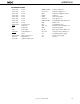
µPD75P3116 FUNCTION OUTLINE Item Instruction execution time • 0.95, 1.91, 3.81, or 15.3 µs (main system clock: @ 4.19 MHz) • 0.67, 1.33, 2.67, or 10.7 µs (main system clock: @ 6.0 MHz) • 122 µs (subsystem clock: @ 32.
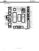
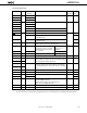
µPD75P3116 CONTENTS 1. PIN CONFIGURATION (TOP VIEW) ................................................................................................. 4 2. BLOCK DIAGRAM ............................................................................................................................ 6 3. PIN FUNCTIONS ............................................................................................................................... 7 3.1 Port Pins ...............................................
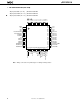
µPD75P3116 1.
µPD75P3116 PIN IDENTIFICATIONS P00 to P03: Port 0 COM0 to COM3: Common output 0 to 3 P10 to P13: Port 1 VLC0 to VLC2: LCD power supply 0 to 2 P20 to P23: Port 2 BIAS: LCD power supply bias control P30 to P33: Port 3 LCDCL: LCD clock P50 to P53: Port 5 SYNC: LCD synchronization P60 to P63: Port 6 TI0 to TI2: Timer input 0 to 2 P80 to P83: Port 8 PTO0 to PTO2: Programmable timer output 0 to 2 P90 to P93: Port 9 BUZ: Buzzer clock KR0 to KR3: Key return 0 to 3 PCL: Programmabl
µPD75P3116 2.
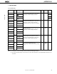
µPD75P3116 3. PIN FUNCTIONS 3.1 Port Pins (1/2) Pin Name P00 I/O Input Alternate Function INT4 Function 4-bit input port (Port 0) Connection of an internal pull-up resistor can be specified by a software setting in 3-bit units.
µPD75P3116 3.1 Port Pins (2/2) Pin Name P60 I/O I/O Alternate Function KR0/D0 P61 KR1/D1 P62 KR2/D2 P63 KR3/D3 P80 I/O S23 P81 S22 P82 S21 P83 S20 P90 I/O S19 P91 S18 P92 S17 P93 S16 Function 8-Bit I/O Status I/O Circuit After Reset TypeNote 1 Programmable 4-bit I/O port (Port 6) Input and output can be specified in 1-bit units. Connection of an internal pull-up resistor can be specified by a software setting in 4-bit units.
µPD75P3116 3.
µPD75P3116 3.
µPD75P3116 3.3 Pin I/O Circuits The I/O circuits for the µPD75P3116’s pins are shown in abbreviated form below. Type A Type D VDD VDD Data P-ch OUT P-ch IN Output disable N-ch N-ch Push-pull output that can be set to high impedance output (with both P-ch and N-ch OFF). CMOS standard input buffer Type B Type E-B VDD P.U.R. P.U.R. enable P-ch IN Data IN/OUT Type D Output disable Type A Schmitt-triggered input with hysteresis characteristics. P.U.R.
µPD75P3116 (Continued) Type F-B Type H VDD P.U.R. P.U.R. enable P-ch Output disable (P) VDD SEG data P-ch Type G-A IN/OUT N-ch P-ch IN/OUT Data Output disable N-ch Data Output disable (N) Type E-B Output disable P.U.R. : Pull-Up Resistor Type G-A Type M-C VDD P-ch N-ch VLC0 VLC1 P.U.R. P-ch N-ch P.U.R. enable P-ch P-ch N-ch IN/OUT OUT SEG data Data N-ch Output disable N-ch P-ch N-ch VLC2 N-ch P.U.R.
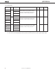
µPD75P3116 3.4 Recommended Connection of Unused Pins Table 3-1. List of Unused Pin Connections Pin Recommended Connection P00/INT4 Connect to Vss or VDD. P01/SCK Input: P02/SO/SB0 Output: Leave open. P03/SI/SB1 Connect to Vss. P10/INT0 and P11/INT1 Connect to Vss or VDD. Independently connect to Vss or VDD via a resistor. P12/TI1/TI2/INT2 P13/TI0 P20/PTO0 Input: Independently connect to Vss or VDD via a resistor. P21/PTO1 Output: Leave open.
µPD75P3116 4. Mk I AND Mk II MODE SELECTION FUNCTION Setting the stack bank selection (SBS) register for the µPD75P3116 enables the program memory to be switched between the Mk I mode and Mk II mode. This function is applicable when using the µPD75P3116 to evaluate the µPD753104, 753106, or 753108.
µPD75P3116 4.2 Setting of Stack Bank Selection (SBS) Register Use the stack bank selection register to switch between the Mk I mode and Mk II mode. Figure 4-1 shows the format of the stack bank selection register. The stack bank selection register is set using a 4-bit memory manipulation instruction. When using the Mk I mode, be sure to initialize the stack bank selection register to 100×BNote at the beginning of the program. When using the Mk II mode, be sure to initialize it to 000×BNote.
µPD75P3116 5. DIFFERENCES BETWEEN µPD75P3116 AND µPD753104, 753106, 753108 The µPD75P3116 replaces the internal mask ROM in the µPD753104, 753106, and 753108 with a one-time PROM and features expanded ROM capacity. The µPD75P3116’s Mk I mode supports the Mk I mode in the µPD753104, 753106, and 753108 and the µPD75P3116’s Mk II mode supports the Mk II mode in the µPD753104, 753106, and 753108. Table 5-1 lists differences between the µPD75P3116 and the µPD753104, 753106, and 753108.
µPD75P3116 6. MEMORY CONFIGURATION Figure 6-1.
µPD75P3116 Figure 6-2. Data Memory Map Data memory Memory bank 000H (32 × 4) General-purpose register area 01FH 020H 0 256 × 4 (224 × 4) Stack areaNote Data area static RAM (512 × 4) 0FFH 100H 256 × 4 (224 × 4) 1DFH 1E0H 1 (24 × 4) Display data memory 1F7H 1F8H (8 × 4) 1FFH Not incorporated F80H 128 × 4 Peripheral hardware area FFFH Note 18 Memory bank 0 or 1 can be selected as the stack area.
µPD75P3116 7. INSTRUCTION SET (1) Representation and coding formats for operands In the instruction’s operand area, use the following coding format to describe operands corresponding to the instruction’s operand representations (for further details, refer to the RA75X Assembler Package Language User’s Manual (U12385E)). When there are several codes, select and use just one. Codes that consist of uppercase letters and + or – symbols are keywords that should be entered as they are.
µPD75P3116 (2) Operation conventions 20 A: A register; 4-bit accumulator B: B register C: C register D: D register E: E register H: H register L: L register X: X register XA: Register pair (XA); 8-bit accumulator BC: Register pair (BC) DE: Register pair (DE) HL: Register pair (HL) XA’: Expansion register pair (XA’) BC’: Expansion register pair (BC’) DE’: Expansion register pair (DE’) HL’: Expansion register pair (HL’) PC: Program counter SP: Stack pointer CY: Carry fla
µPD75P3116 (3) Description of symbols used in addressing area MB = MBE • MBS *1 MBS = 0, 1, 15 *2 MB = 0 MBE = 0: MB = 0 (000H to 07FH) Data memory addressing MB = 15 (F80H to FFFH) *3 MBE = 1: MB = MBS MBS = 0, 1, 15 *4 MB = 15, fmem = FB0H to FBFH, FF0H to FFFH *5 MB = 15, pmem = FC0H to FFFH *6 addr = 0000H to 3FFFH addr, addr1 = (Current PC) – 15 to (Current PC) – 1 *7 (Current PC) + 2 to (Current PC) + 16 caddr = 0000H to 0FFFH (PC13, 12 = 00B) or 1000H to 1FFFH (PC13, 12 = 01B) or *8 2000H
µPD75P3116 Instruction Group Transfer Mnemonic MOV XCH Table reference MOVT Operand No.
µPD75P3116 Instruction Group Bit transfer Arithmetic Mnemonic MOV1 ADDS ADDC SUBS SUBC AND OR XOR Operand No. of Machine Bytes Cycle Operation Addressing Area CY, fmem.bit 2 2 CY ← (fmem.bit) *4 CY, pmem.@L 2 2 CY ← (pmem7-2+L3-2.bit(L1-0)) *5 CY, @H+mem.bit 2 2 CY ← (H+mem3-0.bit) *1 fmem.bit, CY 2 2 (fmem.bit) ← CY *4 pmem.@L, CY 2 2 (pmem7-2+L3-2.bit(L1-0)) ← CY *5 @H+mem.bit, CY 2 2 (H+mem3-0.
µPD75P3116 Instruction Group Comparison Mnemonic SKE Operand No.
µPD75P3116 Instruction Group Branch Mnemonic BRNote 1 Operand BRCB Addressing Area — PC13-0 ← addr Use the assembler to select the most appropriate instruction among the following. • BR !addr • BRCB !caddr • BR $addr *6 — — PC13-0 ← addr1 Use the assembler to select the most appropriate instruction among the following.
µPD75P3116 Instruction Group Subroutine Mnemonic Operand CALLANote !addr1 No.
µPD75P3116 Instruction Group Subroutine Mnemonic 1 (SP–1)(SP–2) ← rp, SP ← SP–2 BS 2 2 (SP–1) ← MBS, (SP–2) ← RBS, SP ← SP–2 rp 1 1 rp ← (SP+1)(SP), SP ← SP+2 BS 2 2 MBS ← (SP+1), RBS ← (SP), SP ← SP+2 2 2 IME(IPS.3) ← 1 2 2 IE××× ← 1 2 2 IME(IPS.
µPD75P3116 8. ONE-TIME PROM (PROGRAM MEMORY) WRITE AND VERIFY The program memory contained in the µPD75P3116 is a 16384 × 8-bit one-time PROM that can be electrically written one time only. The pins listed in the table below are used for this PROM’s write/verify operations. Clock input from the X1 pin is used instead of address input as a method for updating addresses.
µPD75P3116 8.2 Program Memory Write Procedure Program memory can be written at high speed using the following procedure. (1) Pull down unused pins to Vss via resistors. Set the X1 pin to low. (2) Supply 5 V to the VDD and VPP pins. (3) Wait 10 µs. (4) Select the program memory address zero-clear mode. (5) Supply 6 V to VDD and 12.5 V to VPP. (6) Write data in the 1 ms write mode. (7) Select the verify mode. If the data is written, go to (8) and if not, repeat (6) and (7). (8) Additional write.
µPD75P3116 8.3 Program Memory Read Procedure The µPD75P3116 can read program memory contents using the following procedure. (1) Pull down unused pins to VSS via resistors. Set the X1 pin to low. (2) Supply 5 V to the VDD and VPP pins. (3) Wait 10 µs. (4) Select the program memory address zero-clear mode. (5) Supply 6 V to VDD and 12.5 V to VPP. (6) Select the verify mode. Apply four pulses to the X1 pin. The data stored in one address will be output every four clock pulses.
µPD75P3116 8.4 One-Time PROM Screening Due to its structure, the one-time PROM cannot be fully tested before shipment by NEC. Therefore, NEC recommends that after the required data is written and the PROM is stored under the temperature and time conditions shown below, the PROM should be verified via screening. Storage Temperature Storage Time 125˚C 24 hours NEC offers QTOP microcontrollers for which one-time PROM writing, marking, screening, and verification are provided at additional cost.
µPD75P3116 9. ELECTRICAL SPECIFICATIONS Absolute Maximum Ratings (TA = 25˚C) Parameter Symbol Test Conditions Rating Unit Power supply voltage V DD –0.3 to +7.0 V PROM power supply voltage V PP –0.3 to +13.5 V Input voltage V I1 Except port 5 –0.3 to VDD + 0.3 V V I2 Port 5 (N-ch open drain) –0.3 to +14 V –0.3 to VDD + 0.
µPD75P3116 Main System Clock Oscillator Characteristics (TA = –40 to +85°C, VDD = 1.8 to 5.5 V) Resonator Recommended Constant Ceramic MIN. 1.0 TYP. MAX. Unit 6.0Note 2 MHz frequency (fx) Note 1 resonator C1 C2 VDD Crystal Oscillation After V DD reaches oscil- stabilization timeNote 3 lation voltage range MIN. Oscillation X2 X1 4 1.0 ms 6.0Note 2 MHz frequency (fx) Note 1 resonator C1 C2 VDD External Oscillation V DD = 4.5 to 5.5 V 10 stabilization timeNote 3 V DD = 1.8 to 5.
µPD75P3116 Subsystem Clock Oscillator Characteristics (T A = –40 to +85˚C, V DD = 1.8 to 5.5 V) Resonator Recommended Constant Crystal XT1 C3 R frequency (f XT) C4 Oscillation VDD = 4.5 to 5.5 V stabilization time Note 2 VDD = 1.8 to 5.5 V VDD External MIN. TYP. MAX. Unit 32 32.768 35 kHz 1.
µPD75P3116 DC Characteristics (T A = –40 to +85˚C, V DD = 1.8 to 5.5 V) Parameter Output current, low Input voltage, high Symbol I OL VIH1 VIH2 VIH3 Input voltage, low Test Conditions MAX. Unit Per pin 15 mA Total of all pins 150 mA TYP. 2.7 ≤ VDD ≤ 5.5 V 0.7VDD V DD V 1.8 ≤ VDD < 2.7 V 0.9VDD V DD V 2.7 ≤ VDD ≤ 5.5 V 0.8VDD V DD V 1.8 ≤ VDD < 2.7 V 0.9VDD V DD V Port 5 2.7 ≤ VDD ≤ 5.5 V 0.7VDD 13 V (N-ch open-drain) 1.8 ≤ VDD < 2.7 V 0.9VDD 13 V VDD – 0.
µPD75P3116 DC Characteristics (T A = –40 to +85˚C, V DD = 1.8 to 5.5 V) Parameter LCD drive voltage Symbol VLCD VAC0 = 0 Test Conditions MIN. TA = –40 to +85°C TA = –10 to +85°C VAC0 = 1 VAC currentNote 1 I VAC VAC0 = 1, VDD = 2.0 V ±10% LCD output voltage deviationNote 2 (common) VODC lo = ±1.0 µA LCD output voltage deviationNote 2 (segment) VODS Supply current Note 3 I DD1 TYP. MAX. Unit 2.7 V DD V 2.2 V DD V 1.8 V DD V 4 µA 0 ±0.2 V 0 ±0.
µPD75P3116 AC Characteristics (TA = –40 to +85˚C, V DD = 1.8 to 5.5 V) Parameter Symbol CPU clock cycle time t CY Note 1 (Min. instruction execution Test Conditions MIN. TYP. MAX. Unit Operating on VDD = 2.7 to 5.5 V 0.67 64 µs main system clock VDD = 1.8 to 5.5 V 0.95 64 µs 125 µs Operating on subsystem clock 114 122 time = 1 machine cycle) TI0, TI1, TI2 input f TI frequency TI0, TI1, TI2 input t TIH, t TIL high-/low-level width Interrupt input high-/ VDD = 2.7 to 5.
µPD75P3116 Serial Transfer Operation 2-wire and 3-wire serial I/O mode (SCK...Internal clock output): (TA = –40 to +85˚C, VDD = 1.8 to 5.5 V) Parameter SCK cycle time SCK high-/low-level Symbol t KCY1 t KL1, tKH1 width SI Note 1 setup time t SIK1 (to SCK↑) SI Note 1 hold time t KSI1 (from SCK↑) SONote 1 output delay t KSO1 time from SCK↓ Notes 1. 2. Test Conditions MIN. TYP. MAX. Unit VDD = 2.7 to 5.5 V 1300 ns VDD = 1.8 to 5.5 V 3800 ns VDD = 2.7 to 5.5 V t KCY1/2–50 ns VDD = 1.
µPD75P3116 SBI mode (SCK...Internal clock output (master)): (T A = –40 to +85˚C, VDD = 1.8 to 5.5 V) Parameter SCK cycle time SCK high-/low-level Symbol t KCY3 t KL3, t KH3 width SB0, 1 setup time t SIK3 (to SCK↑) SB0, 1 hold time (from SCK↑) t KSI3 SB0, 1 output delay t KSO3 time from SCK↓ Test Conditions MIN. TYP. MAX. Unit VDD = 2.7 to 5.5 V 1300 ns VDD = 1.8 to 5.5 V 3800 ns VDD = 2.7 to 5.5 V tKCY3/2–50 ns VDD = 1.8 to 5.5 V t KCY3/2–150 ns VDD = 2.7 to 5.
µPD75P3116 AC Timing Test Points (Excluding X1, XT1 Input) VIH (MIN.) VIL (MAX.) VIH (MIN.) VIL (MAX.) VOH (MIN.) VOL (MAX.) VOH (MIN.) VOL (MAX.) Clock Timing 1/fX tXL tXH VDD – 0.1 V 0.1 V X1 input 1/fXT tXTL tXTH VDD – 0.1 V 0.
µPD75P3116 Serial Transfer Timing 3-wire serial I/O mode tKCY1, 2 tKL1, 2 tKH1, 2 SCK tSIK1, 2 SI tKSI1, 2 Input data tKSO1, 2 SO Output data 2-wire serial I/O mode tKCY1, 2 tKL1, 2 tKH1, 2 SCK tSIK1, 2 tKSI1, 2 SB0, 1 tKSO1, 2 Data Sheet U11369EJ3V0DS 41
µPD75P3116 Serial Transfer Timing Bus release signal transfer tKCY3, 4 tKL3, 4 tKH3, 4 SCK tKSB tSBL tSBH tSIK3, 4 tSBK SB0, 1 tKSO3, 4 Command signal transfer tKCY3, 4 tKL3, 4 tKH3, 4 SCK tKSB tSIK3, 4 tSBK SB0, 1 tKSO3, 4 Interrupt input timing tINTL tINTH INT0, 1, 2, 4 KR0 to 7 RESET input timing tRSL RESET 42 Data Sheet U11369EJ3V0DS tKSI3, 4 tKSI3, 4
µPD75P3116 Data Memory Stop Mode Low Supply Voltage Data Retention Characteristics (T A = –40 to +85˚C) Parameter Symbol Release signal set time t SREL Oscillation stabilization t WAIT MIN. TYP. MAX. Release by RESET Release by interrupt request Unit µs 0 wait time Note 1 Notes 1. Test Conditions 215 /fX ms Note 2 ms The oscillation stabilization wait time is the time during which the CPU operation is stopped to prevent unstable operation at the start of oscillation. 2.
µPD75P3116 Data Retention Timing (STOP Mode Release by RESET) Internal reset operation HALT mode Operating mode STOP mode Data retention mode VDD tSREL STOP instruction execution RESET tWAIT Data Retention Timing (Standby Release Signal: STOP Mode Release by Interrupt Signal) HALT mode Operating mode STOP mode Data retention mode VDD tSREL STOP instruction execution Standby release signal (Interrupt request) tWAIT 44 Data Sheet U11369EJ3V0DS
µPD75P3116 DC Programming Characteristics (TA = 25 ±5˚C, VDD = 6.0 ±0.25 V, VPP = 12.5 ±0.3 V, VSS = 0 V) Parameter Symbol Input voltage, high Input voltage, low Test Conditions MAX. Unit 0.7V DD V DD V VDD – 0.5 V DD V Except X1 and X2 pins 0 0.3VDD V 0 0.4 V 10 µA VIH1 Except X1 and X2 pins VIH2 X1, X2 VIL1 VIL2 X1, X2 Input leakage current ILI VIN = VIL or V IH Output voltage, high VOH IOH = –1 mA Output voltage, low V OL IOL = 1.
µPD75P3116 Program Memory Write Timing tVPS VPP VPP VDD VDD VDD + 1 VDD tVDS tXH X1 D0/P60 to D3/P60 D4/P50 to D7/P53 Data input Data output tDS tI tDS tDH tDV tXL Data input Data input tDH tDF tAH tAS MD0/P30 tPW tM1R tM0S tOPW MD1/P31 tPCR tM1S tM1H MD2/P32 tM3S tM3H MD3/P33 Program Memory Read Timing tVPS VPP VPP VDD VDD VDD + 1 VDD tVDS tXH X1 tXL D0/P60 to D3/P60 D4/P50 to D7/P53 tDAD tHAD Data output Data output tDV tDFR tI tM3HR MD0/P30 MD1/P31 tPCR MD2/P
µPD75P3116 10. CHARACTERISTIC CURVES (REFERENCE VALUES) IDD vs VDD (Main System Clock: 6.0 MHz Crystal Resonator) (TA = 25°C) 10 5.0 PCC = 0011 PCC = 0010 PCC = 0001 PCC = 0000 1.0 Main system clock HALT mode + 32 kHz oscillation Supply current IDD (mA) 0.5 0.1 Subsystem clock operation mode (SOS.1 = 0) Main system clock STOP mode + 32 kHz oscillation (SOS.1 = 0) and subsystem clock HALT mode (SOS.1 = 0) Main system clock STOP mode + 32 kHz oscillation (SOS.1 = 1) and subsystem clock HALT mode (SOS.
µPD75P3116 IDD vs VDD (Main System Clock: 4.19 MHz Crystal Resonator) (TA = 25°C) 10 5.0 PCC = 0011 PCC = 0010 PCC = 0001 1.0 PCC = 0000 Main system clock HALT mode + 32 kHz oscillation Supply current IDD (mA) 0.5 0.1 Subsystem clock operation mode (SOS.1 = 0) Subsystem clock HALT mode (SOS.1 = 0) and main system clock STOP mode + 32 kHz oscillation (SOS.1 = 0) 0.05 Main system clock STOP mode + 32 kHz oscillation (SOS.1 = 1) and subsystem clock HALT mode (SOS.1 = 1) 0.01 0.
µPD75P3116 11. PACKAGE DRAWINGS 64-PIN PLASTIC QFP (14x14) A B 48 49 33 32 detail of lead end S C D Q 64 1 R 17 16 F J G H I M P K S N S L M NOTE ITEM Each lead centerline is located within 0.15 mm of its true position (T.P.) at maximum material condition. MILLIMETERS A 17.6±0.4 B 14.0±0.2 C 14.0±0.2 D 17.6±0.4 F 1.0 G 1.0 H 0.37 +0.08 -0.07 I J 0.15 0.8 (T.P.) K 1.8±0.2 L 0.8±0.2 M 0.17 +0.08 -0.07 N 0.10 P 2.55±0.1 Q 0.1±0.1 R 5°±5° S 2.85 MAX.
µPD75P3116 64-PIN PLASTIC LQFP (12x12) A B 48 49 33 32 detail of lead end S C D Q 64 R 17 16 1 F G J H I M K P S N S L M NOTE ITEM Each lead centerline is located within 0.13 mm of its true position (T.P.) at maximum material condition. MILLIMETERS A 14.8±0.4 B 12.0±0.2 C 12.0±0.2 D 14.8±0.4 F 1.125 G 1.125 H I 0.32±0.08 0.13 J 0.65 (T.P.) K L 1.4±0.2 0.6±0.2 M 0.17 +0.08 -0.07 N 0.10 P 1.4±0.1 Q 0.125±0.075 R 5°±5° S 1.7 MAX.
µPD75P3116 64-PIN PLASTIC LQFP (14x14) A B 48 49 33 32 detail of lead end S P C D T R 64 1 L 17 16 U Q F G J H I M ITEM K S N M S MILLIMETERS A 17.2±0.2 B 14.0±0.2 C 14.0±0.2 D 17.2±0.2 F 1.0 G 1.0 H 0.37 +0.08 -0.07 I 0.20 J K 0.8 (T.P.) 1.6±0.2 NOTE L 0.8 Each lead centerline is located within 0.20 mm of its true position (T.P.) at maximum material condition. M 0.17 +0.03 -0.06 N 0.10 P 1.4±0.1 Q R 0.127±0.075 +4° 3° -3° S T 1.7 MAX. 0.25 U 0.886±0.
µPD75P3116 12. RECOMMENDED SOLDERING CONDITIONS The µPD75P3116 should be soldered and mounted under the conditions recommended in the table below. For details of recommended soldering conditions, refer to the information document Semiconductor Device Mounting Technology Manual (C10535E). For soldering methods and conditions other than those recommended below, contact an NEC Sales representative. Table 12-1.
µPD75P3116 Table 12-1. Surface Mounting Type Soldering Conditions (2/2) (3) µ PD75P3116GC-8BS: 64-pin plastic LQFP (14 × 14) Soldering Method Soldering Conditions Recommended Condition Symbol Infrared reflow Package peak temperature: 235°C, Time: 30 seconds max. (at 210°C or higher), Count: Twice or less IR35-00-2 VPS Package peak temperature: 215°C, Time: 40 seconds max. (at 200°C or higher), Count: Twice or less VP15-00-2 Wave soldering Solder bath temperature: 260°C max., Time: 10 seconds max.
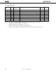
µPD75P3116 APPENDIX A. LIST OF µPD75308B, 753108, AND 75P3116 FUNCTIONS µPD75308B Parameter Program memory Mask ROM 0000H to 1F7FH (8064 × 8 bits) Data memory µ PD753108 Mask ROM 0000H to 1FFFH (8192 × 8 bits) µPD75P3116 One-time PROM 0000H to 3FFFH (16384 × 8 bits) 000H to 1FFH (512 × 4 bits) CPU 75X Standard 75XL CPU • 0.95, 1.91, 3.81, 15.3 µs (during 4.19 MHz operation) • 0.67, 1.33, 2.67, 10.7 µs (during 6.0 MHz operation) Instruction execution time When main system clock is selected 0.
µPD75P3116 µPD75308B Parameter µ PD753108 µPD75P3116 Clock output (PCL) Φ, 524, 262, 65.5 kHz (Main system clock: during 4.19 MHz operation) • Φ, 524, 262, 65.5 kHz (Main system clock: during 4.19 MHz operation) • Φ, 750, 375, 93.8 kHz (Main system clock: during 6.0 MHz operation) BUZ output (BUZ) 2 kHz (Main system clock: during 4.19 MHz operation) • 2, 4, 32 kHz (Main system clock: during 4.19 MHz operation or subsystem clock: during 32.768 kHz operation) • 2.93, 5.86, 46.
µPD75P3116 APPENDIX B. DEVELOPMENT TOOLS The following development tools have been provided for system development using the µPD75P3116. In the 75XL Series, a common relocatable assembler is used in combination with a device file dedicated to each model. RA75X relocatable assembler Host Machine OS PC-9800 Series MS-DOS Supply Medium TM Part Number (Product Name) 3.5" 2HD µS5A13RA75X 3.5" 2HC µS7B13RA75X Ver.3.30 to Ver.6.
µPD75P3116 PROM Write Tools Hardware Software PG-1500 This is a PROM writer that can program a single-chip microcontroller with PROM in stand-alone mode or under the control of a host machine when connected with the supplied accessory board and optional programmer adapter. It can also program typical PROMs in capacities ranging from 256 Kb to 4 Mb. PA-75P3116GC This is a PROM programmer adapter for the µPD75P3116GC-AB8. It can be used when connected to the PG-1500.
µPD75P3116 Debugging Tools An in-circuit emulator (IE-75001-R) is provided as a program debugging tool for the µPD75P3116. The system configuration using this in-circuit emulator is shown below. Hardware IE-75001-R The IE-75001-R is an in-circuit emulator to be used for hardware and software debugging during development of application systems using the 75X or 75XL Series products.
µPD75P3116 OS for IBM PCs The following operating systems for IBM PCs are supported. OS PC DOS TM Version Ver.3.1 to 6.3 J6.1/VNote to J6.3/VNote MS-DOS Ver.5.0 to 6.2 5.0/VNote to 6.2/VNote IBM DOSTM J5.02/VNote Note Only English mode is supported. Caution Ver. 5.0 and later include a task swapping function, but this function cannot be used in this software.
µPD75P3116 Package Drawing and Recommended Footprint of Conversion Socket (EV-9200GC-64) Figure B-1. EV-9200GC-64 Package Drawing (For Reference Only) A N O L K T J C D S F Q M R B E EV-9200GC-64 1 P No.1 pin index G H I EV-9200GC-64-G0E ITEM 60 MILLIMETERS INCHES A 18.8 0.74 B 14.1 0.555 C 14.1 0.555 D 18.8 0.74 E 4-C 3.0 4-C 0.118 F 0.8 0.031 G 6.0 0.236 H 15.8 0.622 I 18.5 0.728 J 6.0 0.236 K 15.8 0.622 L 18.5 0.728 M 8.0 0.315 N 7.8 0.
µPD75P3116 Figure B-2. EV-9200GC-64 Recommended Footprint (For Reference Only) G J H E D F K I L C B A EV-9200GC-64-P1E ITEM MILLIMETERS A 19.5 B 14.8 INCHES 0.768 0.583 C 0.8±0.02 × 15=12.0±0.05 D +0.003 0.8±0.02 × 15=12.0±0.05 0.031+0.002 –0.001 × 0.591=0.472 –0.002 0.031+0.002 –0.001 × 0.591=0.472 +0.003 –0.002 E 14.8 0.583 F 19.5 0.768 G 6.00 ± 0.08 0.236 +0.004 –0.003 H 6.00 ± 0.08 0.236 +0.004 –0.003 I 0.5 ± 0.02 0.197 +0.001 –0.002 J φ 2.36 ± 0.03 φ 0.093 +0.
µPD75P3116 Package Drawing of Conversion Adapter (TGK-064SBW) Figure B-3. TGK-064SBW Package Drawing (For Reference Only) A B K L X M C T G F E D H I J Protrusion height U S V Q W R N O P a Z e Y d k j h i c b f g ITEM A 62 MILLIMETERS 18.4 INCHES ITEM MILLIMETERS INCHES 0.724 a φ 0.3 φ 0.012 B 0.65x15=9.75 0.026x0.591=0.384 b 1.85 0.073 C 0.65 0.026 c 3.5 0.138 D 7.75 0.305 d 2.0 0.079 E F 10.15 12.55 0.400 0.494 e f 3.9 1.325 0.154 0.052 G 14.
µPD75P3116 Notes on Target System Design The following shows a diagram of the connection conditions between the emulation probe, conversion connector and conversion socket or conversion adapter. Design your system making allowances for conditions such as the form of parts mounted on the target system, as shown below. Table B-1.
µPD75P3116 Figure B-6. Connection Conditions of Target System (1) Ground clip 64-pin GC EP-753108GC-R In-circuit emulator IE-75001-R External sense clips 8 mm 35 mm 18.5 mm Conversion socket EV-9200GC-64 35 mm 18.5 mm Target system Figure B-7. Connection Conditions of Target System (2) Ground clip 64-pin GK EP-753108GK-R In-circuit emulator IE-75001-R 9 mm External sense clips Notch Conversion adapter TGK-064SBW 13.8 mm 34 mm 18.4 mm 34 mm 18.
µPD75P3116 APPENDIX C. RELATED DOCUMENTS The related documents indicated in this publication may include preliminary versions. However, preliminary versions are not marked as such. Documents Related to Devices Document Name Document No.
µPD75P3116 Other Related Documents Document Name Document No. SEMICONDUCTOR SELECTION GUIDE – Products & Packages – X13769E Semiconductor Device Mounting Technology Manual C10535E Quality Grades on NEC Semiconductor Devices C11531E NEC Semiconductor Device Reliability/Quality Control System C10983E Guide to Prevent Damage for Semiconductor Devices by Electrostatic Discharge (ESD) C11892E Caution The related documents listed above are subject to change without notice.
µPD75P3116 [MEMO] Data Sheet U11369EJ3V0DS 67
µPD75P3116 NOTES FOR CMOS DEVICES 1 PRECAUTION AGAINST ESD FOR SEMICONDUCTORS Note: Strong electric field, when exposed to a MOS device, can cause destruction of the gate oxide and ultimately degrade the device operation. Steps must be taken to stop generation of static electricity as much as possible, and quickly dissipate it once, when it has occurred. Environmental control must be adequate. When it is dry, humidifier should be used.
µPD75P3116 Regional Information Some information contained in this document may vary from country to country. Before using any NEC product in your application, pIease contact the NEC office in your country to obtain a list of authorized representatives and distributors.
µPD75P3116 QTOP is a trademark of NEC Corporation. MS-DOS is either a registered trademark or a trademark of Microsoft Corporation in the United States and/or other countries. IBM DOS, PC/AT, and PC DOS are trademarks of International Business Machines Corporation. The export of this product from Japan is regulated by the Japanese government. To export this product may be prohibited without governmental license, the need for which must be judged by the customer.