
Information


Document: NWP01, Version 1.0 4/8
frequencies the impedance of BNC connectors
became more important than ever.
Every deviate impedance has a negative influ-
ence on the "return loss“ / "VSWR“ (Voltage
Standing Wave Ratio) which are important
measurements for reflected signals in a trans-
mission line.
Especially on high frequencies - as they occur
when transmitting high frame rate HD signals
(typical transmission @ 4.5 GHz) - an imped-
ance mismatch results in a lot of return loss.
3.3 How To Measure Return Loss
Return loss is measured by the help of a Net-
work Analyzer. The analyzer is set to nominal
cable impedance (e.g. 75 Ω) and the tested ca-
ble is terminated with a 75 Ω load. A signal is
introduced to the cable and the reflected signal
is measured.
4 Timing Jitter
4.1 What Is Jitter?
This simple and intuitive definition is provided by
the SONET specification
2
:
“Jitter is defined as the short-term variations of a
digital signal’s significant instants from their ideal
positions in time.”
Ideally, the time interval between transitions in
an SDI signal should equal an integer multiple of
the unit interval. In real systems, however, the
transitions in an SDI signal can vary from their
ideal locations in time. This variation is called
time interval error (TIE), commonly referred to as
jitter. This timing variation can be induced by a
variety of frequency, amplitude, and phase-
related effects.
4.2 Wander, Timing Jitter
The jitter spectrum in an actual SDI signal gen-
erally contains a range of spectral components.
The recovered clock will generally track spectral
components below the clock recovery band-
width, but will not track spectral components
above this bandwidth.
Hence, the impact of jitter on decoding depends
on both the jitter’s amplitude and its frequency
components. This has led to a frequency-based
classification of jitter.
Conventionally, the term “jitter” refers to short-
term time interval error, i.e. spectral components
above some low frequency threshold. For SDI
signals, the SMPTE standards set this threshold
at 10 Hz and refer to spectral components above
this frequency as timing jitter.
The term wander refers to long-term time interval
error. For SDI signals, components in the jitter
spectrum below 10 Hz are classified as wander.
4.3 About Timing Jitter
Timing jitter has always degraded electrical sys-
tems, but the drive to higher data rates and lower
logic swings has focused increasing interest and
concern on it.
Impedance discontinuities through connectors
and transmission lines as well as attenuation,
cross talk, and noise coupling contribute to jitter.
In all of the above cases, the jitter effect is due to
some form of signal distortion and cannot be
completely eliminated. Thus, the jitter introduced
from these effects can be considered systematic
and cumulative (arithmetically additive).
4.4 How To Measure Timing Jitter
Various methods to measure and estimate peak-
peak jitter are common in industry.
We decided to use the eye diagram, which is a
general tool for jitter measurement, since it gives
insight into the amplitude behavior of the wave-
form as well as the timing behavior.
4.4.1 The Eye Diagram
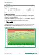
4
Figure 1
An eye diagram is created when many short
segments of a waveform are superimposed such
that the nominal edge locations and voltage lev-
els are aligned, as suggested in stylized Figure 1
(Colours have been used to show how the indi-
vidual waveform segments are composed into an
eye diagram).
The waveform segments may be adjacent ones,
as shown in the figure, or may be taken from
more widely spaced samples of the signal.
Figure 2
Colored eye diagrams are used to indicate the
density of waveform samples at any given point
of the display. Figure 2 shows such a color den-
sity display for a waveform that exhibits several
types of noise.
As the jitter on a signal increases, the eye be-
comes less open, either horizontally, vertically or
both. The eye is said to be closed when no open
area remains in the center of the diagram.
Ideal
Sampling
Point
Unit Interval(UI)
Jitter Jitter