
Data Sheet
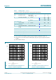
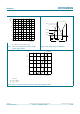
Table Of Contents

©
Nexperia B.V. 2017. All rights reserved
2N7002BKS All information provided in this document is subject to legal disclaimers.
Product data sheet Rev. 2 — 23 September 2010 3 of 16
Nexperia
2N7002BKS
60 V, 300 mA dual N-channel Trench MOSFET
[1] Device mounted on an FR4 PCB, single-sided copper, tin-plated, mounting pad for drain 1 cm
2
.
[2] Device mounted on an FR4 Printed-Circuit Board (PCB), single-sided copper, tin-plated and standard
footprint.
[3] Measured between all pins.
I
DM
peak drain current T
amb
=25°C;
single pulse; t
p
≤ 10 μs
-1.2A
P
tot
total power dissipation T
amb
=25°C
[2]
-295mW
[1]
-340mW
T
sp
=25°C - 1040 mW
Source-drain diode
I
S
source current T
amb
=25°C
[1]
-300mA
ESD maximum rating
V
ESD
electrostatic discharge
voltage
human body model
[3]
- 2000 V
Per device
P
tot
total power dissipation T
amb
=25°C
[2]
-445mW
T
j
junction temperature 150 °C
T
amb
ambient temperature −55 +150 °C
T
stg
storage temperature −65 +150 °C
Table 5. Limiting values …continued
In accordance with the Absolute Maximum Rating System (IEC 60134).
Symbol Parameter Conditions Min Max Unit
Fig 1. Normalized total power dissipation as a
function of ambient temperature
Fig 2. Normalized continuous drain current as a
function of ambient temperature
T
amb
(°C)
−75 17512525 75−25
017aaa001
40
80
120
P
der
(%)
0
T
amb
(°C)
−75 17512525 75−25
017aaa002
40
80
120
I
der
(%)
0
P
der
P
tot
P
tot 25°C()
------------------------
100 %×= I
der
I
D
I
D25°C()
--------------------
100 %×=