
Data Sheet
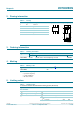
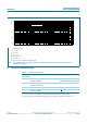
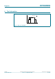
Table Of Contents

©
Nexperia B.V. 2017. All rights reserved
2N7002BKS All information provided in this document is subject to legal disclaimers.
Product data sheet Rev. 2 — 23 September 2010 4 of 16
Nexperia
2N7002BKS
60 V, 300 mA dual N-channel Trench MOSFET
6. Thermal characteristics
[1] Device mounted on an FR4 PCB, single-sided copper, tin-plated and standard footprint.
[2] Device mounted on an FR4 PCB, single-sided copper, tin-plated, mounting pad for drain 1 cm
2
.
I
DM
= single pulse
(1) t
p
= 100 μs
(2) t
p
=1ms
(3) t
p
=10ms
(4) DC; T
sp
=25°C
(5) t
p
= 100 ms
(6) DC; T
amb
=25°C; drain mounting pad 1 cm
2
Fig 3. Safe operating area; junction to ambient; continuous and peak drain currents as a function of
drain-source voltage
017aaa056
10
−1
10
−2
1
10
I
D
(A)
10
−3
V
DS
(V)
10
−1
10
2
101
(1)
(2)
(3)
(4)
(5)
(6)
Limit R
DSon
= V
DS
/I
D
Table 6. Thermal characteristics
Symbol Parameter Conditions Min Typ Max Unit
Per transistor
R
th(j-a)
thermal resistance from
junction to ambient
in free air
[1]
- 370 425 K/W
[2]
- 320 370 K/W
R
th(j-sp)
thermal resistance from
junction to solder point
- - 120 K/W
Per device
R
th(j-a)
thermal resistance from
junction to ambient
in free air
[1]
- - 275 K/W