
Data Sheet


74AHC_AHCT574_2
Product data sheet Rev. 02 — 24 January 2008 10 of 18
Nexperia
74AHC574; 74AHCT574
Octal D-type flip-flop; positive edge-trigger; 3-state
[1] Typical values are measured at nominal supply voltage (V
CC
= 3.3 V and V
CC
= 5.0 V).
[2] t
pd
is the same as t
PLH
and t
PHL
.
t
en
is the same as t
PZL
and t
PZH
.
t
dis
is the same as t
PLZ
and t
PHZ
.
[3] C
PD
is used to determine the dynamic power dissipation P
D
(µW).
P
D
=C
PD
× V
CC
2
× f
i
+ ∑ (C
L
× V
CC
2
× f
o
) where:
f
i
= input frequency in MHz;
f
o
= output frequency in MHz;
C
L
= output load capacitance in pF;
V
CC
= supply voltage in V.
10.1 Waveforms
t
h
hold time Dn to CP; see Figure 8
V
CC
= 4.5 V to 5.5 V;
C
L
=50pF
1.5 - - 1.5 - 1.5 - ns
C
PD
power
dissipation
capacitance
per buffer;
C
L
=50pF;f=1 MHz;
V
I
= GND to V
CC
[3]
-12- - - - -pF
Table 7. Dynamic characteristics
…continued
GND = 0 V. For test circuit see Figure 10.
Symbol Parameter Conditions 25 °C −40 °C to +85 °C −40 °C to +125 °C Unit
Min Typ
[1]
Max Min Max Min Max
Measurement points are given in Table 8.
V
OL
and V
OH
are typical voltage output levels that occur with the output load.
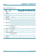
Fig 7. Propagation delay input (CP) to output (Qn), clock input (CP) pulse width and the maximum frequency
(CP)
mna802
CP
input
Qn
output
t
PHL
t
PLH
t
W
1/f
max
V
M
V
OH
V
I
GND
V
OL
V
M
©
Nexperia B.V. 2017. All rights reserved