74HC04; 74HCT04 Hex inverter Rev. 5 — 27 November 2015 Product data sheet 1. General description The 74HC04; 74HCT04 is a hex inverter. The inputs include clamp diodes that enable the use of current limiting resistors to interface inputs to voltages in excess of VCC. 2.
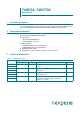
74HC04; 74HCT04 Nexperia Hex inverter 4. Functional diagram $ < $ < $ < $ < $ < $ < PQD Fig 1. < $ PQD Logic symbol Fig 2. PQD IEC logic symbol Fig 3.
74HC04; 74HCT04 Nexperia Hex inverter 5.1 Pin description Table 2. Pin description Symbol Pin Description 1A, 2A, 3A, 4A, 5A, 6A 1, 3, 5, 9, 11, 13 data input 1Y, 2Y, 3Y, 4Y, 5Y, 6Y 2, 4, 6, 8, 10, 12 data output GND 7 ground (0 V) VCC 14 supply voltage 6. Functional description Table 3. Function table H = HIGH voltage level; L = LOW voltage level Input Output nA nY L H H L 7. Limiting values Table 4.
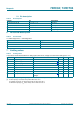
74HC04; 74HCT04 Nexperia Hex inverter 8. Recommended operating conditions Table 5. Recommended operating conditions Voltages are referenced to GND (ground = 0 V) Symbol Parameter Conditions 74HC04 Min Typ 74HCT04 Max Min Typ Unit Max VCC supply voltage 2.0 5.0 6.0 4.5 5.0 5.5 V VI input voltage 0 - VCC 0 - VCC V VO output voltage 0 - VCC 0 - VCC V Tamb ambient temperature 40 +25 +125 40 +25 +125 C t/V input transition rise and fall rate VCC = 2.
74HC04; 74HCT04 Nexperia Hex inverter Table 6. Static characteristics …continued At recommended operating conditions; voltages are referenced to GND (ground = 0 V). Symbol Parameter CI 25 C Conditions input capacitance 40 C to +85 C 40 C to +125 C Unit Min Typ Max Min Max Min Max - 3.5 - - - - - pF 74HCT04 VIH HIGH-level input voltage VCC = 4.5 V to 5.5 V 2.0 1.6 - 2.0 - 2.0 - V VIL LOW-level input voltage VCC = 4.5 V to 5.5 V - 1.2 0.8 - 0.8 - 0.
74HC04; 74HCT04 Nexperia Hex inverter Table 7. Dynamic characteristics …continued GND = 0 V; CL = 50 pF; for test circuit see Figure 7. Symbol Parameter CPD power dissipation capacitance 25 C Conditions 40 C to +125 C Unit Min Typ Max Max (85 C) Max (125 C) - 21 - - - VCC = 4.5 V - 10 19 24 29 ns VCC = 5.
4HC04; 74HCT04 Nexperia Hex inverter 9, QHJDWLYH SXOVH W: 90 90 *1' WI 9, WI SRVLWLYH SXOVH *1' WU WU 90 90 W: 9&& * 9, 92 '87 57 &/ DDK Test data is given in Table 9. Definitions test circuit: RT = termination resistance should be equal to output impedance Zo of the pulse generator. CL = load capacitance including jig and probe capacitance. Fig 7. Table 9.
74HC04; 74HCT04 Nexperia Hex inverter 12.
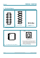
74HC04; 74HCT04 Nexperia Hex inverter 6623 SODVWLF VKULQN VPDOO RXWOLQH SDFNDJH OHDGV ERG\ ZLGWK PP ' 627 ( $ ; F \ + ( Y 0 $ = 4 $ $ $ $ SLQ LQGH[ ș / S / GHWDLO ; Z 0 E S H PP VFDOH ',0(16,216 PP DUH WKH RULJLQDO GLPHQVLRQV 81,7 $ PD[ $ $ $ E S F ' ( H + ( / / S 4 Y Z \ = ș PP
74HC04; 74HCT04 Nexperia Hex inverter 76623 SODVWLF WKLQ VKULQN VPDOO RXWOLQH SDFNDJH OHDGV ERG\ ZLGWK PP ' 627 ( $ ; F \ + ( Y 0 $ = 4 $ SLQ LQGH[ $ $ $ ș / S / H GHWDLO ; Z 0 E S PP VFDOH ',0(16,216 PP DUH WKH RULJLQDO GLPHQVLRQV 81,7 $ PD[ $ $ $ E S F ' ( H + ( / / S 4 Y Z \ = ș PP
74HC04; 74HCT04 Nexperia Hex inverter '+94)1 SODVWLF GXDO LQ OLQH FRPSDWLEOH WKHUPDO HQKDQFHG YHU\ WKLQ TXDG IODW SDFNDJH QR OHDGV WHUPLQDOV ERG\ [ [ PP % ' 627 $ $ $ ( F GHWDLO ; WHUPLQDO LQGH[ DUHD WHUPLQDO LQGH[ DUHD & H H Y Z E & $ % & \ \ & / (K H N 'K ; N PP VFDOH 'LPHQVLRQV PP DUH WKH RULJLQDO GLPHQVLRQV 8QLW PP PD[ QRP PLQ $ $ E F ' 'K ( (K H H
74HC04; 74HCT04 Nexperia Hex inverter 13. Abbreviations Table 10. Abbreviations Acronym Description CMOS Complementary Metal-Oxide Semiconductor DUT Device Under Test ESD ElectroStatic Discharge HBM Human Body Model MM Machine Model TTL Transistor-Transistor Logic 14. Revision history Table 11. Revision history Document ID Release date Data sheet status Change notice Supersedes 74HC_HCT04 v.5 20151127 Product data sheet - 74HC_HCT04 v.4 Modifications: 74HC_HCT04 v.
74HC04; 74HCT04 Nexperia Hex inverter 15. Legal information 15.1 Data sheet status Document status[1][2] Product status[3] Definition Objective [short] data sheet Development This document contains data from the objective specification for product development. Preliminary [short] data sheet Qualification This document contains data from the preliminary specification. Product [short] data sheet Production This document contains the product specification.
74HC04; 74HCT04 Nexperia Hex inverter Export control — This document as well as the item(s) described herein may be subject to export control regulations. Export might require a prior authorization from competent authorities. Non-automotive qualified products — Unless this data sheet expressly states that this specific Nexperia product is automotive qualified, the product is not suitable for automotive use.
Nexperia 74HC04; 74HCT04 Hex inverter 17. Contents 1 2 3 4 5 5.1 6 7 8 9 10 11 12 13 14 15 15.1 15.2 15.3 15.4 16 17 © General description . . . . . . . . . . . . . . . . . . . . . . 1 Features and benefits . . . . . . . . . . . . . . . . . . . . 1 Ordering information . . . . . . . . . . . . . . . . . . . . . 1 Functional diagram . . . . . . . . . . . . . . . . . . . . . . 2 Pinning information . . . . . . . . . . . . . . . . . . . . . . 2 Pin description . . . . . . . . . . . . . . . . . . . . . . . .