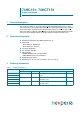
74HC151; 74HCT151 8-input multiplexer Rev. 6 — 28 December 2015 Product data sheet 1. General description The 74HC151; 74HCT151 are 8-bit multiplexer with eight binary inputs (I0 to I7), three select inputs (S0 to S2) and an enable input (E). One of the eight binary inputs is selected by the select inputs and routed to the complementary outputs (Y and Y). A HIGH on E forces the output Y LOW and output Y HIGH.
74HC151; 74HCT151 Nexperia 8-input multiplexer 4. Functional diagram Fig 1. , , , , , , , , < < ( 6 6 6 DDD Logic symbol , , , , , , , , , , , 6 6 , , < , < , 08/7,3/(;(5 6 , ( < < DDD Fig 2. Functional diagram 74HC_HCT151 Product data sheet 6 Fig 3.
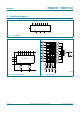
74HC151; 74HCT151 Nexperia 8-input multiplexer 5. Pinning information 5.1 Pinning +& +&7 , , 9&& , , , , , < , < 6 ( 6 *1' 6 DDD Fig 4. Pin configuration SO16 and (T)SSOP16 5.2 Pin description Table 2.
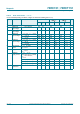
74HC151; 74HCT151 Nexperia 8-input multiplexer 6. Functional description Function table[1] Table 3.
74HC151; 74HCT151 Nexperia 8-input multiplexer Table 4. Limiting values …continued In accordance with the Absolute Maximum Rating System (IEC 60134). Voltages are referenced to GND (ground = 0 V). Symbol Parameter Conditions Ptot total power dissipation Tamb = 40 C to +125 C Min Max Unit SO16 package [1] - 500 mW (T)SSOP16 package [2] - 500 mW [1] For SO16 package: Ptot derates linearly with 8 mW/K above 70 C. [2] For SSOP16 and TSSOP16 packages: Ptot derates linearly with 5.
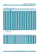
74HC151; 74HCT151 Nexperia 8-input multiplexer 9. Static characteristics Table 6. Static characteristics At recommended operating conditions; voltages are referenced to GND (ground = 0 V). Symbol Parameter Tamb = 25 C Conditions Min Typ VCC = 2.0 V 1.5 VCC = 4.5 V 3.15 VCC = 6.0 V 4.2 VCC = 2.0 V - VCC = 4.5 V - VCC = 6.0 V Tamb = 40 C to +85 C Tamb = 40 C to Unit +125 C Max Min Max Min Max 1.2 - 1.5 - 1.5 - V 2.4 - 3.15 - 3.15 - V 3.2 - 4.2 - 4.2 - V 0.
4HC151; 74HCT151 Nexperia 8-input multiplexer Table 6. Static characteristics …continued At recommended operating conditions; voltages are referenced to GND (ground = 0 V). Symbol Parameter Tamb = 25 C Conditions Min Typ Tamb = 40 C to +85 C Tamb = 40 C to Unit +125 C Max Min Max Min Max 74HCT151 VIH HIGH-level input voltage VCC = 4.5 V to 5.5 V 2.0 1.6 - 2.0 - 2.0 - V VIL LOW-level input voltage VCC = 4.5 V to 5.5 V - 1.2 0.8 - 0.8 - 0.
74HC151; 74HCT151 Nexperia 8-input multiplexer 10. Dynamic characteristics Table 7. Dynamic characteristics Voltages are referenced to GND (ground = 0 V); CL = 50 pF unless otherwise specified; for test circuit see Figure 7. Symbol Parameter Tamb = 25 C Conditions Tamb = 40 C to +85 C Tamb = 40 C to +125 C Unit Min Typ Max Min Max Min Max VCC = 2.0 V - 52 170 - 215 - 255 ns VCC = 4.
74HC151; 74HCT151 Nexperia 8-input multiplexer Table 7. Dynamic characteristics …continued Voltages are referenced to GND (ground = 0 V); CL = 50 pF unless otherwise specified; for test circuit see Figure 7. Symbol Parameter CPD power dissipation capacitance Tamb = 25 C Conditions Tamb = 40 C to +85 C Tamb = 40 C to +125 C Unit Min Typ Max Min Max Min Max - 40 - - - - - pF - 22 38 - 48 - 57 ns - 19 - - - - - ns VCC = 4.
74HC151; 74HCT151 Nexperia 8-input multiplexer 11. Waveforms 9, 90 ,Q LQSXW 90 *1' W3+/ 92+ W3/+ 90 < RXWSXW 90 92/ W7/+ W7+/ W3/+ 92+ 90 < RXWSXW 92/ W3+/ 90 W7/+ W7+/ DDD Measurement points are given in Table 8. VOL and VOH are typical voltage output levels that occur with the output load. Fig 5.
74HC151; 74HCT151 Nexperia 8-input multiplexer Table 8. Measurement points Type Input Output VM VM 74HC151 0.5VCC 0.5VCC 74HCT151 1.3 V 1.3 V 9, QHJDWLYH SXOVH W: 90 *1' 9, WI WU WU WI SRVLWLYH SXOVH *1' 90 90 90 W: 9&& * 9, 92 '87 57 &/ DDK Test data is given in Table 9. Definitions test circuit: RT = Termination resistance should be equal to output impedance Zo of the pulse generator.
74HC151; 74HCT151 Nexperia 8-input multiplexer 12.
74HC151; 74HCT151 Nexperia 8-input multiplexer 6623 SODVWLF VKULQN VPDOO RXWOLQH SDFNDJH OHDGV ERG\ ZLGWK PP ' 627 ( $ ; F \ + ( Y 0 $ = 4 $ $ $ $ SLQ LQGH[ ș / S / GHWDLO ; Z 0 E S H PP VFDOH ',0(16,216 PP DUH WKH RULJLQDO GLPHQVLRQV 81,7 $ PD[ $ $ $ E S F ' ( H + ( / / S 4 Y Z \ = ș PP
74HC151; 74HCT151 Nexperia 8-input multiplexer 76623 SODVWLF WKLQ VKULQN VPDOO RXWOLQH SDFNDJH OHDGV ERG\ ZLGWK PP ' 627 ( $ ; F \ + ( Y 0 $ = 4 $ SLQ LQGH[ $ $ $ ș / S / H GHWDLO ; Z 0 E S PP VFDOH ',0(16,216 PP DUH WKH RULJLQDO GLPHQVLRQV 81,7 $ PD[ $ $ $ E S F ' ( H + ( / / S 4 Y Z \ = ș PP
74HC151; 74HCT151 Nexperia 8-input multiplexer 13. Abbreviations Table 10. Abbreviations Acronym Description CMOS Complementary Metal Oxide Semiconductor DUT Device Under Test ESD ElectroStatic Discharge HBM Human Body Model MM Machine Model TTL Transistor-Transistor Logic 14. Revision history Table 11. Revision history Document ID Release date Data sheet status Change notice Supersedes 74HC_HCT151 v.6 20151228 Product data sheet - 74HC_HCT151 v.5 Modifications: 74HC_HCT151 v.
74HC151; 74HCT151 Nexperia 8-input multiplexer 15. Legal information 15.1 Data sheet status Document status[1][2] Product status[3] Definition Objective [short] data sheet Development This document contains data from the objective specification for product development. Preliminary [short] data sheet Qualification This document contains data from the preliminary specification. Product [short] data sheet Production This document contains the product specification.
74HC151; 74HCT151 Nexperia 8-input multiplexer Export control — This document as well as the item(s) described herein may be subject to export control regulations. Export might require a prior authorization from competent authorities. Non-automotive qualified products — Unless this data sheet expressly states that this specific Nexperia product is automotive qualified, the product is not suitable for automotive use.
Nexperia 74HC151; 74HCT151 8-input multiplexer 17. Contents 1 2 3 4 5 5.1 5.2 6 7 8 9 10 11 12 13 14 15 15.1 15.2 15.3 15.4 16 17 © General description . . . . . . . . . . . . . . . . . . . . . . 1 Features and benefits . . . . . . . . . . . . . . . . . . . . 1 Ordering information . . . . . . . . . . . . . . . . . . . . . 1 Functional diagram . . . . . . . . . . . . . . . . . . . . . . 2 Pinning information . . . . . . . . . . . . . . . . . . . . . . 3 Pinning . . . . . . . . . . . . . . . . . . . . .