74HC257; 74HCT257 Quad 2-input multiplexer; 3-state Rev. 7 — 2 February 2016 Product data sheet 1. General description The 74HC257; 74HCT257 is a quad 2-input multiplexer with 3-state outputs. Inputs include clamp diodes. This enables the use of current limiting resistors to interface inputs to voltages in excess of VCC. 2. Features and benefits Non-inverting data path 3-state outputs interface directly with system bus Complies with JEDEC standard no.
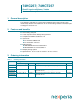
74HC257; 74HCT257 Nexperia Quad 2-input multiplexer; 3-state 4. Functional diagram , , , , , , , , 2( 6 < < * (1 < < DDG Logic symbol Fig 2. , , 6 2( Fig 3. PJD Fig 1.
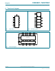
74HC257; 74HCT257 Nexperia Quad 2-input multiplexer; 3-state , < , , < , , < , , < , 2( 6 Fig 4. DDG Logic diagram 5. Pinning information 5.1 Pinning +& +&7 6 9&& , 2( , , < , , < , , < , *1' < DDG Fig 5. Pin configuration SO16, SSOP16 and TSSOP16 74HC_HCT257 Product data sheet All information provided in this document is subject to legal disclaimers. . Rev.
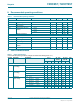
74HC257; 74HCT257 Nexperia Quad 2-input multiplexer; 3-state 5.2 Pin description Table 2. Pin description Symbol Pin Description S 1 common data select input 1I0 to 4I0 2, 5, 11, 14 data input from source 0 1I1 to 4I1 3, 6, 10, 13 data input from source 1 1Y to 4Y 4, 7, 9, 12 3-state multiplexer output GND 8 ground (0 V) OE 15 3-state output enable input (active LOW) VCC 16 supply voltage 6. Functional description 6.1 Function table Table 3.
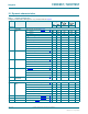
74HC257; 74HCT257 Nexperia Quad 2-input multiplexer; 3-state 8. Recommended operating conditions Table 5. Recommended operating conditions Symbol Parameter Conditions Min Typ Max Unit 74HC257 VCC supply voltage 2.0 5.0 6.0 V VI input voltage 0 - VCC V VO output voltage 0 - VCC V t/V input transition rise and fall rates VCC = 2.0 V - - 625 ns VCC = 4.5 V - 1.67 139 ns VCC = 6.
74HC257; 74HCT257 Nexperia Quad 2-input multiplexer; 3-state Table 6. Static characteristics …continued At recommended operating conditions; voltages are referenced to GND (ground = 0 V). Symbol Parameter Conditions VOL VI = VIH or VIL LOW-level output voltage 25 C 40 C to +85 C 40 C to +125 C Unit Min Typ Max Min Max Min Max IO = 20 A; VCC = 2.0 V - 0 0.1 - 0.1 - 0.1 V IO = 20 A; VCC = 4.5 V - 0 0.1 - 0.1 - 0.1 V IO = 20 A; VCC = 6.0 V - 0 0.1 - 0.
4HC257; 74HCT257 Nexperia Quad 2-input multiplexer; 3-state 10. Dynamic characteristics Table 7. Dynamic characteristics Voltages are referenced to GND (ground = 0 V); For test circuit see Figure 8. Symbol Parameter 25 C Conditions 40 C to +85 C 40 C to Unit +125 C Typ Max Max Max 74HC257 tpd propagation delay nl0 to nY or nl1 to nY; see Figure 6 [1] VCC = 2.0 V 36 110 140 165 ns VCC = 4.5 V 13 22 28 33 ns VCC = 5.0 V; CL = 15 pF 11 - - - ns VCC = 6.
74HC257; 74HCT257 Nexperia Quad 2-input multiplexer; 3-state Table 7. Dynamic characteristics …continued Voltages are referenced to GND (ground = 0 V); For test circuit see Figure 8. Symbol Parameter power dissipation per multiplexer; VI = GND to VCC 1.5 V capacitance CPD [1] 40 C to +85 C 40 C to Unit +125 C Typ Max Max Max 45 - - - [5] pF tpd is the same as tPHL, tPLH. [2] ten is the same as tPZH, tPZL. [3] tdis is the same as tPHZ, tPLZ. [4] tt is the same as tTHL, tTLH.
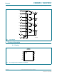
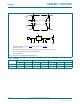
74HC257; 74HCT257 Nexperia Quad 2-input multiplexer; 3-state WU 9, WI 2( LQSXW 90 *1' W3/= RXWSXW W3=/ 9&& /2: WR 2)) 2)) WR /2: 90 92/ W3+= RXWSXW 92+ W3=+ +,*+ WR 2)) 2)) WR +,*+ *1' 90 RXWSXWV HQDEOHG RXWSXWV HQDEOHG RXWSXWV GLVDEOHG DDF Measurement points are given in Table 8. VOL and VOH are typical voltage output levels that occur with the output load. Fig 7. 3-state output enable and disable times Table 8.
74HC257; 74HCT257 Nexperia Quad 2-input multiplexer; 3-state 9, W: QHJDWLYH SXOVH 90 9 WI WU WU WI 9, SRVLWLYH SXOVH 9 90 90 90 W: 9&& 9&& * 9, 92 5/ 6 RSHQ '87 &/ 57 DDG Measurement points are given in Table 8 and test data is given in Table 9. Definitions test circuit: RT = Termination resistance should be equal to output impedance Zo of the pulse generator. CL = Load capacitance including jig and probe capacitance. RL = Load resistance.
74HC257; 74HCT257 Nexperia Quad 2-input multiplexer; 3-state 12.
74HC257; 74HCT257 Nexperia Quad 2-input multiplexer; 3-state 6623 SODVWLF VKULQN VPDOO RXWOLQH SDFNDJH OHDGV ERG\ ZLGWK PP ' 627 ( $ ; F \ + ( Y 0 $ = 4 $ $ $ $ SLQ LQGH[ ș / S / GHWDLO ; Z 0 E S H PP VFDOH ',0(16,216 PP DUH WKH RULJLQDO GLPHQVLRQV 81,7 $ PD[ $ $ $ E S F ' ( H + ( / / S 4 Y Z \ = ș PP
74HC257; 74HCT257 Nexperia Quad 2-input multiplexer; 3-state 76623 SODVWLF WKLQ VKULQN VPDOO RXWOLQH SDFNDJH OHDGV ERG\ ZLGWK PP ' 627 ( $ ; F \ + ( Y 0 $ = 4 $ SLQ LQGH[ $ $ $ ș / S / H GHWDLO ; Z 0 E S PP VFDOH ',0(16,216 PP DUH WKH RULJLQDO GLPHQVLRQV 81,7 $ PD[ $ $ $ E S F ' ( H + ( / / S 4 Y Z \ = ș PP
74HC257; 74HCT257 Nexperia Quad 2-input multiplexer; 3-state 13. Abbreviations Table 10. Abbreviations Acronym Description CMOS Complementary Metal Oxide Semiconductor DUT Device Under Test ESD ElectroStatic Discharge HBM Human Body Model MM Machine Model TTL Transistor-Transistor Logic 14. Revision history Table 11. Revision history Document ID Release date Data sheet status Change notice Supersedes 74HC_HCT257 v.7 20160202 Product data sheet - Modifications: 74HC_HCT257 v.
74HC257; 74HCT257 Nexperia Quad 2-input multiplexer; 3-state 15. Legal information 15.1 Data sheet status Document status[1][2] Product status[3] Definition Objective [short] data sheet Development This document contains data from the objective specification for product development. Preliminary [short] data sheet Qualification This document contains data from the preliminary specification. Product [short] data sheet Production This document contains the product specification.
74HC257; 74HCT257 Nexperia Quad 2-input multiplexer; 3-state Export control — This document as well as the item(s) described herein may be subject to export control regulations. Export might require a prior authorization from competent authorities. Non-automotive qualified products — Unless this data sheet expressly states that this specific Nexperia product is automotive qualified, the product is not suitable for automotive use.
Nexperia 74HC257; 74HCT257 Quad 2-input multiplexer; 3-state 17. Contents 1 2 3 4 5 5.1 5.2 6 6.1 7 8 9 10 11 12 13 14 15 15.1 15.2 15.3 15.4 16 17 © General description . . . . . . . . . . . . . . . . . . . . . . 1 Features and benefits . . . . . . . . . . . . . . . . . . . . 1 Ordering information . . . . . . . . . . . . . . . . . . . . . 1 Functional diagram . . . . . . . . . . . . . . . . . . . . . . 2 Pinning information . . . . . . . . . . . . . . . . . . . . . . 3 Pinning . . . . . . . . . . . .