74HC27; 74HCT27 Triple 3-input NOR gate Rev. 5.1 — 27 November 2015 Product data sheet 1. General description The 74HC27; 74HCT27 is a triple 3-input NOR gate. Inputs include clamp diodes. This enables the use of current limiting resistors to interface inputs to voltages in excess of VCC. 2. Features and benefits Complies with JEDEC standard no.
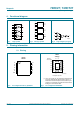
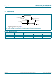
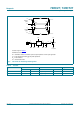
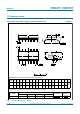
74HC27; 74HCT27 Nexperia Triple 3-input NOR gate 4. Functional diagram $ % & $ % & $ % & < $ < % & PQD PQD Fig 1. < < Logic symbol Fig 2. IEC logic symbol PQD Fig 3. Logic diagram (one gate) 5. Pinning information 5.
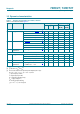
74HC27; 74HCT27 Nexperia Triple 3-input NOR gate 5.2 Pin description Table 2. Pin description Symbol Pin Description 1A, 2A, 3A 1, 3, 9 data input 1B, 2B, 3B 2, 4, 10 data input 1C, 2C, 3C 13, 5, 11 data input 1Y, 2Y, 3Y 12, 6, 8 data output GND 7 ground (0 V) VCC 14 supply voltage 6. Functional description Table 3. Function table[1] Inputs Outputs nA nB nC nY L L L H X X H L X H X L H X X L [1] H = HIGH voltage level; L = LOW voltage level; X = don’t care.
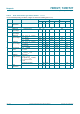
74HC27; 74HCT27 Nexperia Triple 3-input NOR gate 8. Recommended operating conditions Table 5. Recommended operating conditions Voltages are referenced to GND (ground = 0 V) Symbol Parameter Conditions 74HC27 Min Typ 74HCT27 Max Min Typ Unit Max VCC supply voltage 2.0 5.0 6.0 4.5 5.0 5.
74HC27; 74HCT27 Nexperia Triple 3-input NOR gate Table 6. Static characteristics type 74HC27; 74HCT27 …continued At recommended operating conditions; voltages are referenced to GND (ground = 0 V). Symbol Parameter CI 25 C Conditions input capacitance 40 C to +85 C 40 C to +125 C Unit Min Typ Max Min Max Min Max - 3.5 - - - - - pF 74HCT27 VIH HIGH-level input voltage VCC = 4.5 V to 5.5 V 2.0 1.6 - 2.0 - 2.0 - V VIL LOW-level input voltage VCC = 4.5 V to 5.5 V - 1.
74HC27; 74HCT27 Nexperia Triple 3-input NOR gate 10. Dynamic characteristics Table 7. Dynamic characteristics type 74HC27; 74HCT27 GND = 0 V; for load circuit see Figure 7. Symbol Parameter 25 C Conditions 40 C to +125 C Unit Min Typ Max Max (85 C) Max (125 C) - 28 90 115 135 VCC = 4.5 V - 10 18 23 27 ns VCC = 5.0 V; CL = 15 pF - 8 - - - ns - 8 15 20 23 ns VCC = 2.0 V - 19 75 95 110 ns VCC = 4.
4HC27; 74HCT27 Nexperia Triple 3-input NOR gate 11. Waveforms 9, Q$ Q% Q& LQSXW 90 *1' W3+/ 92+ W3/+ 9< 90 9; Q< RXWSXW 92/ W7+/ W7/+ DDJ Measurement points are given in Table 8. VOL and VOH are typical voltage output drop that occur with the output load. Fig 6. Table 8. Input (nA, nB, nC) to output (nY) propagation delays and output transition times Measurement points Type Input Output VM VM VX VY 74HC27 0.5VCC 0.5VCC 0.1VCC 0.9VCC 74HCT27 1.3 V 1.3 V 0.1VCC 0.
74HC27; 74HCT27 Nexperia Triple 3-input NOR gate 9, W: QHJDWLYH SXOVH 90 9 WI WU WU WI 9, SRVLWLYH SXOVH 9 90 90 90 W: 9&& 9&& * 9, 92 5/ 6 RSHQ '87 &/ 57 DDG Test data is given in Table 9. Definitions test circuit: RT = Termination resistance should be equal to output impedance Zo of the pulse generator. CL = Load capacitance including jig and probe capacitance. RL = Load resistance. S1 = Test selection switch Fig 7. Table 9.
74HC27; 74HCT27 Nexperia Triple 3-input NOR gate 12.
74HC27; 74HCT27 Nexperia Triple 3-input NOR gate 6623 SODVWLF VKULQN VPDOO RXWOLQH SDFNDJH OHDGV ERG\ ZLGWK PP ' 627 ( $ ; F \ + ( Y 0 $ = 4 $ $ $ $ SLQ LQGH[ ș / S / GHWDLO ; Z 0 E S H PP VFDOH ',0(16,216 PP DUH WKH RULJLQDO GLPHQVLRQV 81,7 $ PD[ $ $ $ E S F ' ( H + ( / / S 4 Y Z \ = ș PP
74HC27; 74HCT27 Nexperia Triple 3-input NOR gate 76623 SODVWLF WKLQ VKULQN VPDOO RXWOLQH SDFNDJH OHDGV ERG\ ZLGWK PP ' 627 ( $ ; F \ + ( Y 0 $ = 4 $ SLQ LQGH[ $ $ $ ș / S / H GHWDLO ; Z 0 E S PP VFDOH ',0(16,216 PP DUH WKH RULJLQDO GLPHQVLRQV 81,7 $ PD[ $ $ $ E S F ' ( H + ( / / S 4 Y Z \ = ș PP
74HC27; 74HCT27 Nexperia Triple 3-input NOR gate '+94)1 SODVWLF GXDO LQ OLQH FRPSDWLEOH WKHUPDO HQKDQFHG YHU\ WKLQ TXDG IODW SDFNDJH QR OHDGV WHUPLQDOV ERG\ [ [ PP % ' 627 $ $ $ ( F GHWDLO ; WHUPLQDO LQGH[ DUHD WHUPLQDO LQGH[ DUHD & H H Y Z E & $ % & \ \ & / (K H N 'K ; N PP VFDOH 'LPHQVLRQV PP DUH WKH RULJLQDO GLPHQVLRQV 8QLW PP PD[ QRP PLQ $ $ E F ' 'K ( (K H
74HC27; 74HCT27 Nexperia Triple 3-input NOR gate 13. Abbreviations Table 10. Abbreviations Acronym Description CMOS Complementary Metal Oxide Semiconductor DUT Device Under Test ESD ElectroStatic Discharge HBM Human Body Model MM Machine Model TTL Transistor-Transistor Logic 14. Revision history Table 11. Revision history Document ID Release date Data sheet status Change notice Supersedes 74HC_HCT27 v.5.1 20151127 Product data sheet - 74HC_HCT27 v.5 - 74HC_HCT27 v.
74HC27; 74HCT27 Nexperia Triple 3-input NOR gate 15. Legal information 15.1 Data sheet status Document status[1][2] Product status[3] Definition Objective [short] data sheet Development This document contains data from the objective specification for product development. Preliminary [short] data sheet Qualification This document contains data from the preliminary specification. Product [short] data sheet Production This document contains the product specification.
74HC27; 74HCT27 Nexperia Triple 3-input NOR gate Export control — This document as well as the item(s) described herein may be subject to export control regulations. Export might require a prior authorization from competent authorities. Non-automotive qualified products — Unless this data sheet expressly states that this specific Nexperia product is automotive qualified, the product is not suitable for automotive use.
Nexperia 74HC27; 74HCT27 Triple 3-input NOR gate 17. Contents 1 2 3 4 5 5.1 5.2 6 7 8 9 10 11 12 13 14 15 15.1 15.2 15.3 15.4 16 17 © General description . . . . . . . . . . . . . . . . . . . . . . 1 Features and benefits . . . . . . . . . . . . . . . . . . . . 1 Ordering information . . . . . . . . . . . . . . . . . . . . . 1 Functional diagram . . . . . . . . . . . . . . . . . . . . . . 2 Pinning information . . . . . . . . . . . . . . . . . . . . . . 2 Pinning . . . . . . . . . . . . . . . . . . . .