74HC4052; 74HCT4052 Dual 4-channel analog multiplexer/demultiplexer Rev. 12 — 10 October 2017 1 Product data sheet General description The 74HC4052; 74HCT4052 is a dual single-pole quad-throw analog switch (2x SP4T) suitable for use in analog or digital 4:1 multiplexer/demultiplexer applications. Each switch features four independent inputs/outputs (nY0, nY1, nY2 and nY3) and a common input/output (nZ). A digital enable input (E) and two digital select inputs (S0 and S1) are common to both switches.
74HC4052; 74HCT4052 Nexperia Dual 4-channel analog multiplexer/demultiplexer 4 Ordering information Table 1. Ordering information Type number 74HC4052D Package Temperature range Name Description Version -40 °C to +125 °C SO16 plastic small outline package; 16 leads; body width 3.9 mm SOT109-1 -40 °C to +125 °C SSOP16 plastic shrink small outline package; 16 leads; body width 5.3 mm SOT338-1 -40 °C to +125 °C TSSOP16 plastic thin shrink small outline package; 16 leads; body width 4.
74HC4052; 74HCT4052 Nexperia Dual 4-channel analog multiplexer/demultiplexer nYn VCC VEE VCC VCC VCC VEE VEE from logic nZ mnb043 Figure 3. Schematic diagram (one switch) VDD 16 13 12 14 15 S0 10 11 S1 E 9 LOGIC LEVEL CONVERSION 1Z 1Y0 1Y1 1Y2 1Y3 1-OF-4 DECODER 1 2Y0 6 5 2 4 8 7 VSS VEE 3 2Y1 2Y2 2Y3 2Z 001aah872 Figure 4. Functional diagram 74HC_HCT4052 Product data sheet All information provided in this document is subject to legal disclaimers. Rev.
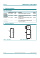
74HC4052; 74HCT4052 Nexperia Dual 4-channel analog multiplexer/demultiplexer 6 Pinning information 6.1 Pinning 2Y0 1 terminal 1 index area 2Y2 2 15 1Y2 2Z 3 14 1Y1 2Y3 4 13 1Z 2Y1 5 12 1Y0 2Y2 2 15 1Y2 E 6 2Z 3 14 1Y1 VEE 7 2Y3 4 13 1Z 2Y1 5 12 1Y0 E 6 11 1Y3 VEE 7 10 S0 GND 8 9 VCC(1) 11 1Y3 10 S0 9 16 VCC 8 1 S1 2Y0 GND 74HC4052 74HCT4052 16 VCC 74HC4052 74HCT4052 001aah823 Transparent top view (1) This is not a supply pin.
74HC4052; 74HCT4052 Nexperia Dual 4-channel analog multiplexer/demultiplexer 7 Functional description Table 3. Function table [1] Input Channel on E S1 S0 L L L nY0 and nZ L L H nY1 and nZ L H L nY2 and nZ L H H nY3 and nZ H X X none [1] H = HIGH voltage level; L = LOW voltage level; X = don’t care. 8 Limiting values Table 4. Limiting values In accordance with the Absolute Maximum Rating System (IEC 60134). Voltages are referenced to VEE = GND (ground = 0 V).
74HC4052; 74HCT4052 Nexperia Dual 4-channel analog multiplexer/demultiplexer 9 Recommended operating conditions Table 5. Recommended operating conditions Symbol Parameter VCC Conditions supply voltage 74HC4052 74HCT4052 Unit Min Typ Max Min Typ Max VCC - GND 2.0 5.0 10.0 4.5 5.0 5.5 V VCC - VEE 2.0 5.0 10.0 2.0 5.0 10.
4HC4052; 74HCT4052 Nexperia Dual 4-channel analog multiplexer/demultiplexer 10 Static characteristics Table 6. RON resistance per switch for 74HC4052 and 74HCT4052 VI = VIH or VIL; for test circuit see Figure 9. Vis is the input voltage at a nYn or nZ terminal, whichever is assigned as an input. Vos is the output voltage at a nYn or nZ terminal, whichever is assigned as an output. For 74HC4052: VCC - GND or VCC - VEE = 2.0 V, 4.5 V, 6.0 V and 9.0 V. For 74HCT4052: VCC - GND = 4.5 V and 5.
74HC4052; 74HCT4052 Nexperia Dual 4-channel analog multiplexer/demultiplexer Symbol Parameter Conditions Min [1] Typ Max Unit Tamb = -40 °C to +125 °C Vis = VCC to VEE RON(peak) ON resistance (peak) [2] VCC = 2.0 V; VEE = 0 V; ISW = 100 μA RON(rail) - - - Ω VCC = 4.5 V; VEE = 0 V; ISW = 1000 μA - - 270 Ω VCC = 6.0 V; VEE = 0 V; ISW = 1000 μA - - 240 Ω VCC = 4.5 V; VEE = -4.5 V; ISW = 1000 μA - - 195 Ω - - - Ω VCC = 4.5 V; VEE = 0 V; ISW = 1000 μA - - 210 Ω VCC = 6.
74HC4052; 74HCT4052 Nexperia Dual 4-channel analog multiplexer/demultiplexer Table 7. Static characteristics for 74HC4052 Voltages are referenced to GND (ground = 0 V). Vis is the input voltage at pins nYn or nZ, whichever is assigned as an input. Vos is the output voltage at pins nZ or nYn, whichever is assigned as an output. Symbol Parameter [1] Conditions Min Typ Max Unit VCC = 2.0 V 1.5 1.2 - V VCC = 4.5 V 3.15 2.4 - V VCC = 6.0 V 4.2 3.2 - V VCC = 9.0 V 6.3 4.
74HC4052; 74HCT4052 Nexperia Dual 4-channel analog multiplexer/demultiplexer Symbol Parameter [1] Conditions Min Typ Max Unit VCC = 2.0 V 1.5 - - V VCC = 4.5 V 3.15 - - V VCC = 6.0 V 4.2 - - V VCC = 9.0 V 6.3 - - V VCC = 2.0 V - - 0.5 V VCC = 4.5 V - - 1.35 V VCC = 6.0 V - - 1.8 V VCC = 9.0 V - - 2.7 V VCC = 6.0 V - - ±1.0 μA VCC = 10.0 V - - ±2.0 μA per channel - - ±1.0 μA all channels - - ±2.0 μA - - ±2.0 μA VCC = 6.0 V - - 160.
74HC4052; 74HCT4052 Nexperia Dual 4-channel analog multiplexer/demultiplexer Table 8. Static characteristics for 74HCT4052 Voltages are referenced to GND (ground = 0 V). Vis is the input voltage at pins nYn or nZ, whichever is assigned as an input. Vos is the output voltage at pins nZ or nYn, whichever is assigned as an output. Symbol Parameter Conditions Min Typ [1] Max Unit Tamb = -40 °C to +85 °C VIH HIGH-level input voltage VCC = 4.5 V to 5.5 V 2.0 1.
74HC4052; 74HCT4052 Nexperia Dual 4-channel analog multiplexer/demultiplexer Symbol Parameter Conditions Min Typ [1] Max Unit Tamb = -40 °C to +125 °C VIH HIGH-level input voltage VCC = 4.5 V to 5.5 V 2.0 - - V VIL LOW-level input voltage VCC = 4.5 V to 5.5 V - - 0.8 V II input leakage current VI = VCC or GND; VCC = 5.5 V; VEE = 0 V - - ±1.0 μA IS(OFF) OFF-state leakage current VCC = 10.0 V; VEE = 0 V; VI = VIH or VIL; |VSW| = VCC - VEE; see Figure 11 per channel - - ±1.
74HC4052; 74HCT4052 Nexperia Dual 4-channel analog multiplexer/demultiplexer 11 Dynamic characteristics Table 9. Dynamic characteristics for 74HC4052 GND = 0 V; tr = tf = 6 ns; CL = 50 pF; for test circuit see Figure 15. Vis is the input voltage at a nYn or nZ terminal, whichever is assigned as an input. Vos is the output voltage at a nYn or nZ terminal, whichever is assigned as an output.
74HC4052; 74HCT4052 Nexperia Dual 4-channel analog multiplexer/demultiplexer Symbol Parameter Conditions Min [1] Typ Max Unit Tamb = -40 °C to +125 °C propagation delay Vis to Vos; RL = ∞ Ω; see Figure 13 tpd ton turn-on time [2] VCC = 2.0 V; VEE = 0 V - - 90 ns VCC = 4.5 V; VEE = 0 V - - 18 ns VCC = 6.0 V; VEE = 0 V - - 15 ns VCC = 4.5 V; VEE = -4.5 V - - 12 ns VCC = 2.0 V; VEE = 0 V - - 490 ns VCC = 4.5 V; VEE = 0 V - - 98 ns VCC = 6.
74HC4052; 74HCT4052 Nexperia Dual 4-channel analog multiplexer/demultiplexer Table 10. Dynamic characteristics for 74HCT4052 GND = 0 V; tr = tf = 6 ns; CL = 50 pF; for test circuit see Figure 15. Vis is the input voltage at a nYn or nZ terminal, whichever is assigned as an input. Vos is the output voltage at a nYn or nZ terminal, whichever is assigned as an output.
74HC4052; 74HCT4052 Nexperia Dual 4-channel analog multiplexer/demultiplexer 50 % Vis input tPLH tPHL 50 % Vos output 001aad555 Figure 13. Input (Vis) to output (Vos) propagation delays VI E, Sn inputs VM 0V tPZL tPLZ 50 % Vos output 10 % tPHZ tPZH 90 % 50 % Vos output switch ON switch OFF switch ON 001aae330 For 74HC4052: VM = 0.5 × VCC. For 74HCT4052: VM = 1.3 V. Figure 14.
74HC4052; 74HCT4052 Nexperia Dual 4-channel analog multiplexer/demultiplexer tW VI 90 % negative pulse VM VM 10 % 0V VI tf tr tr tf 90 % positive pulse VM VM 10 % 0V tW VCC Vis PULSE GENERATOR VI VCC Vos RL DUT RT S1 open CL GND VEE 001aae382 Definitions for test circuit; see Table 11: RT = Termination resistance should be equal to the output impedance Zo of the pulse generator. CL = Load capacitance including jig and probe capacitance. RL = Load resistance.
74HC4052; 74HCT4052 Nexperia Dual 4-channel analog multiplexer/demultiplexer 12 Additional dynamic characteristics Table 12. Additional dynamic characteristics Recommended conditions and typical values; GND = 0 V; Tamb = 25 °C; CL = 50 pF. Vis is the input voltage at pins nYn or nZ, whichever is assigned as an input. Vos is the output voltage at pins nYn or nZ, whichever is assigned as an output.
74HC4052; 74HCT4052 Nexperia Dual 4-channel analog multiplexer/demultiplexer VCC Sn 0.1 µF Vis nYn/nZ nZ/nYn VEE GND RL Vos CL dB 001aah871 VCC = 4.5 V; GND = 0 V; VEE = -4.5 V; RL = 600 Ω; RS = 1 kΩ. a. Test circuit 001aae332 0 α iso (dB) - 20 - 40 - 60 - 80 - 100 102 10 103 104 105 fi (kHz) 106 b. Isolation (OFF-state) as a function of frequency Figure 17. Test circuit for measuring isolation (OFF-state) VCC Sn Vis 0.
74HC4052; 74HCT4052 Nexperia Dual 4-channel analog multiplexer/demultiplexer 2RL 2RL VCC Sn, E Vct nYn G 2RL nZ VEE GND oscilloscope 2RL 001aah913 Figure 19. Test circuit for measuring crosstalk between control input and any switch VCC Sn Vis 10 µF nYn/nZ nZ/nYn VEE GND RL Vos CL dB 001aah829 VCC = 4.5 V; GND = 0 V; VEE = -4.5 V; RL = 50 Ω; RS = 1 kΩ. a. Test circuit 001aad551 5 Vos (dB) 3 1 -1 -3 -5 10 102 103 104 105 f (kHz) 106 b.
74HC4052; 74HCT4052 Nexperia Dual 4-channel analog multiplexer/demultiplexer 13 Package outline SO16: plastic small outline package; 16 leads; body width 3.9 mm SOT109-1 D E A X c y HE v M A Z 16 9 Q A2 A (A 3) A1 pin 1 index θ Lp 1 L 8 e w M bp 0 2.5 detail X 5 mm scale DIMENSIONS (inch dimensions are derived from the original mm dimensions) UNIT A max. A1 A2 A3 bp c D (1) E (1) e HE L Lp Q v w y Z (1) mm 1.75 0.25 0.10 1.45 1.25 0.25 0.49 0.36 0.25 0.
74HC4052; 74HCT4052 Nexperia Dual 4-channel analog multiplexer/demultiplexer SSOP16: plastic shrink small outline package; 16 leads; body width 5.3 mm D SOT338-1 E A X c y HE v M A Z 9 16 Q A2 A (A 3) A1 pin 1 index θ Lp L 8 1 detail X w M bp e 0 2.5 5 mm scale DIMENSIONS (mm are the original dimensions) UNIT A max. A1 A2 A3 bp c D (1) E (1) e HE L Lp Q v w y Z (1) θ mm 2 0.21 0.05 1.80 1.65 0.25 0.38 0.25 0.20 0.09 6.4 6.0 5.4 5.2 0.65 7.9 7.6 1.25 1.
74HC4052; 74HCT4052 Nexperia Dual 4-channel analog multiplexer/demultiplexer TSSOP16: plastic thin shrink small outline package; 16 leads; body width 4.4 mm D SOT403-1 E A X c y HE v M A Z 9 16 Q A2 pin 1 index (A 3 ) A1 A θ Lp 1 L 8 detail X w M bp e 0 2.5 5 mm scale DIMENSIONS (mm are the original dimensions) UNIT A max. A1 A2 A3 bp c D (1) E (2) e HE L Lp Q v w y Z (1) θ mm 1.1 0.15 0.05 0.95 0.80 0.25 0.30 0.19 0.2 0.1 5.1 4.9 4.5 4.3 0.65 6.6 6.
74HC4052; 74HCT4052 Nexperia Dual 4-channel analog multiplexer/demultiplexer DHVQFN16: plastic dual in-line compatible thermal enhanced very thin quad flat package; no leads; SOT763-1 16 terminals; body 2.5 x 3.5 x 0.85 mm B D A A E A1 c detail X terminal 1 index area terminal 1 index area C e1 e b 2 y y1 C v M C A B w M C 7 L 1 8 Eh e 16 9 15 10 Dh X 0 2.5 5 mm scale DIMENSIONS (mm are the original dimensions) UNIT A(1) max.
74HC4052; 74HCT4052 Nexperia Dual 4-channel analog multiplexer/demultiplexer 14 Abbreviations Table 13. Abbreviations Acronym Description CMOS Complementary Metal Oxide Semiconductor DUT Device Under Test ESD ElectroStatic Discharge HBM Human Body Model MM Machine Model 15 Revision history Table 14. Revision history Document ID Release date Data sheet status Change notice Supersedes 74HC_HCT4052 v.12 20171010 Product data sheet - 74HC_HCT4052 v.
74HC4052; 74HCT4052 Nexperia Dual 4-channel analog multiplexer/demultiplexer 16 Legal information 16.1 Data sheet status Document status [1][2] Product status [3] Definition Objective [short] data sheet Development This document contains data from the objective specification for product development. Preliminary [short] data sheet Qualification This document contains data from the preliminary specification.
74HC4052; 74HCT4052 Nexperia Dual 4-channel analog multiplexer/demultiplexer Non-automotive qualified products — Unless this data sheet expressly states that this specific Nexperia product is automotive qualified, the product is not suitable for automotive use. It is neither qualified nor tested in accordance with automotive testing or application requirements. Nexperia accepts no liability for inclusion and/or use of non-automotive qualified products in automotive equipment or applications.
Nexperia 74HC4052; 74HCT4052 Dual 4-channel analog multiplexer/demultiplexer Contents 1 2 3 4 5 6 6.1 6.2 7 8 9 10 11 12 13 14 15 16 General description ............................................ 1 Features and benefits .........................................1 Applications .........................................................1 Ordering information .......................................... 2 Functional diagram ............................................. 2 Pinning information ..................