
Data Sheet

©
Nexperia B.V. 2017. All rights reserved
74HC_HCT245 All information provided in this document is subject to legal disclaimers.
Product data sheet Rev. 4 — 26 February 2016 3 of 18
Nexperia
74HC245; 74HCT245
Octal bus transceiver; 3-state
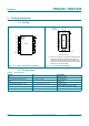
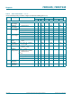
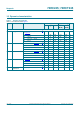
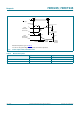
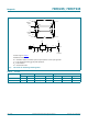
5. Pinning information
5.1 Pinning
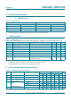
5.2 Pin description
(1) This is not a supply pin. The substrate is attached to this
pad using conductive die attach material. There is no
electrical or mechanical requirement to solder this pad.
However, if it is soldered, the solder land should remain
floating or be connected to GND.
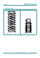
Fig 3. Pin configuration SO20 and (T)SSOP20 Fig 4. Pin configuration DHVQFN20
',5 9
&&
$ 2(
$ %
$ %
$ %
$ %
$ %
$ %
$ %
*1' %
DDF
DDF
*1'
7UDQVSDUHQWWRSYLHZ
%
$
$
%
$ %
$ %
$ %
$ %
$ %
$ 2(
*1'
%
',5
9
&&
WHUPLQDO
LQGH[DUHD
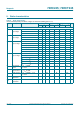
Table 2. Pin description
Symbol Pin Description
DIR 1 direction control
A0, A1, A2, A3, A4, A5, A6, A7 2, 3, 4, 5, 6, 7, 8, 9 data input/output
GND 10 ground (0 V)
B7, B6, B5, B4, B3, B2, B1, B0 11, 12, 13, 14, 15, 16, 17, 18 data input/output
OE
19 output enable input (active LOW)
V
CC
20 supply voltage