74HC597; 74HCT597 8-bit shift register with input flip-flops Rev. 4 — 25 February 2016 Product data sheet 1. General description The 74HC597; 74HCT597 is an 8-bit shift register with input flip-flops. It consists of an 8-bit storage register feeding a parallel-in, serial-out 8-bit shift register. Both the storage register and the shift register have positive edge-triggered clocks. The shift register also has direct load (from storage) and clear inputs.
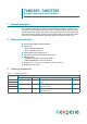
74HC597; 74HCT597 Nexperia 8-bit shift register with input flip-flops 4. Functional diagram 67&3 ' ' ' ' ' ' ' ' 05 '6 67&3 05 '6 ' ' ' ' ' ' ' ' ,1387 )/,3 )/236 %,7 6+,)7 5(*,67(5 3/ 4 ,1387 )/,3 )/236 6+&3 %,7 6+,)7 5(*,67(5 3/ 6+&3 DDD Fig 1. 4 DDD Functional diagram Fig 2.
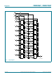
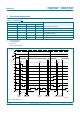
74HC597; 74HCT597 Nexperia 8-bit shift register with input flip-flops 05 6+&3 3/ 67&3 '6 ' & 6 ' ' & ' 5 & 6 6 5 ' & ' 5 & 6 6 5 ' & ' 5 & 6 6 5 ' & ' 5 & 6 6 5 ' & ' 5 & 6 6 5 ' & ' 5 & 6 6 5 ' & ' 5 & 6 5 6 ' 4 & 5 DDD Fig 4. Logic diagram 74HC_HCT597 Product data sheet All information provided in this document is subject to legal disclaimers. Rev. 4 — 25 February 2016 © Nexperia B.V. 2017.
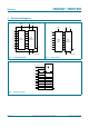
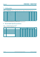
74HC597; 74HCT597 Nexperia 8-bit shift register with input flip-flops 5. Pinning information 5.1 Pinning +& +&7 ' ' 9&& ' ' '6 ' 3/ ' 67&3 ' 6+&3 ' 05 *1' 4 DDD Fig 5. Pin configuration SO16, SSOP16 and TSSOP16 5.2 Pin description Table 2.
74HC597; 74HCT597 Nexperia 8-bit shift register with input flip-flops 6. Functional description Function table[1] Table 3.
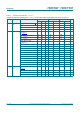
74HC597; 74HCT597 Nexperia 8-bit shift register with input flip-flops 7. Limiting values Table 4. Limiting values In accordance with the Absolute Maximum Rating System (IEC 60134). Voltages are referenced to GND (ground = 0 V). Symbol Parameter VCC supply voltage IIK input clamping current IOK output clamping current IO output current ICC Min Max 0.5 +7 V VI < 0.5 V or VI > VCC + 0.5 V - 20 mA VO < 0.5 V or VO > VCC + 0.5 V - 20 mA VO = 0.5 V to (VCC + 0.
4HC597; 74HCT597 Nexperia 8-bit shift register with input flip-flops 9. Static characteristics Table 6. Static characteristics At recommended operating conditions; voltages are referenced to GND (ground = 0 V). Symbol Parameter 25 C Conditions Min Typ VCC = 2.0 V 1.5 VCC = 4.5 V VCC = 6.0 V 40 C to +85 C 40 C to +125 C Unit Max Min Max Min Max 1.2 - 1.5 - 1.5 - V 3.15 2.4 - 3.15 - 3.15 - V 4.2 3.2 - 4.2 - 4.
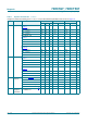
74HC597; 74HCT597 Nexperia 8-bit shift register with input flip-flops Table 6. Static characteristics …continued At recommended operating conditions; voltages are referenced to GND (ground = 0 V). Symbol Parameter 25 C Conditions Min Typ Max Min Max Min Max - - 8.0 - 80.0 - 160.0 A per input pin; DS input - 25 90 - 112.5 - 122.
74HC597; 74HCT597 Nexperia 8-bit shift register with input flip-flops Table 7. Dynamic characteristics …continued Voltages are referenced to GND (ground = 0 V); CL = 50 pF unless otherwise specified; for test circuit, see Figure 13. Symbol Parameter tt tW transition time pulse width 25 C Conditions 40 C to +85 C 40 C to +125 C Unit Min Typ Max Min Max Min Max [2] see Figure 9 VCC = 2.0 V - 19 75 - 95 - 110 ns VCC = 4.5 V - 7 15 - 19 - 22 ns VCC = 6.
74HC597; 74HCT597 Nexperia 8-bit shift register with input flip-flops Table 7. Dynamic characteristics …continued Voltages are referenced to GND (ground = 0 V); CL = 50 pF unless otherwise specified; for test circuit, see Figure 13. Symbol Parameter tsu set-up time 25 C Conditions 40 C to +85 C 40 C to +125 C Unit Min Typ Max Min Max Min Max VCC = 2.0 V 60 8 - 75 - 90 - ns VCC = 4.5 V 12 3 - 15 - 18 - ns VCC = 6.0 V 10 2 - 13 - 15 - ns VCC = 2.
74HC597; 74HCT597 Nexperia 8-bit shift register with input flip-flops Table 7. Dynamic characteristics …continued Voltages are referenced to GND (ground = 0 V); CL = 50 pF unless otherwise specified; for test circuit, see Figure 13.
74HC597; 74HCT597 Nexperia 8-bit shift register with input flip-flops Table 7. Dynamic characteristics …continued Voltages are referenced to GND (ground = 0 V); CL = 50 pF unless otherwise specified; for test circuit, see Figure 13.
74HC597; 74HCT597 Nexperia 8-bit shift register with input flip-flops 9, 90 05 LQSXW *1' W: W3+/ 92+ 4 RXWSXW 90 92/ DDD Measurement points are given in Table 8. VOL and VOH are typical voltage output levels that occur with the output load. Fig 8. input (MR) to (Q), output propagation delays and (MR) pulse width IPD[ 9, 90 3/ LQSXW *1' W: W3/+ W3+/ 92+ 4 RXWSXW 90 92/ W7+/ W7/+ DDD Measurement points are given in Table 8.
74HC597; 74HCT597 Nexperia 8-bit shift register with input flip-flops 9, SRVLWLYH '6 'Q LQSXW 90 *1' 9, QHJDWLYH '6 'Q LQSXW 90 *1' WVX WK 9, 90 6+&3 LQSXW *1' 9, 90 67&3 LQSXW *1' WVX WK DDD Measurement points are given in Table 8. Fig 11. Hold and set-up times for (DS), (Dn) inputs to (SHCP), (STCP) inputs 9, 3/ LQSXW 90 *1' 9, 90 6+&3 LQSXW *1' WVX WK DDD Measurement points are given in Table 8. Fig 12. Set-up times for (PL) input to (SHCP) input Table 8.
74HC597; 74HCT597 Nexperia 8-bit shift register with input flip-flops 9, W: QHJDWLYH SXOVH 90 9 WI WU WU WI 9, SRVLWLYH SXOVH 9 90 90 90 W: 9&& 9&& * 9, 92 5/ 6 RSHQ '87 &/ 57 DDG Test data is given in Table 9. Definitions test circuit: RT = Termination resistance should be equal to output impedance Zo of the pulse generator. CL = Load capacitance including jig and probe capacitance. RL = Load resistance. S1 = Test selection switch. Fig 13.
74HC597; 74HCT597 Nexperia 8-bit shift register with input flip-flops 12.
74HC597; 74HCT597 Nexperia 8-bit shift register with input flip-flops 6623 SODVWLF VKULQN VPDOO RXWOLQH SDFNDJH OHDGV ERG\ ZLGWK PP ' 627 ( $ ; F \ + ( Y 0 $ = 4 $ $ $ $ SLQ LQGH[ ș / S / GHWDLO ; Z 0 E S H PP VFDOH ',0(16,216 PP DUH WKH RULJLQDO GLPHQVLRQV 81,7 $ PD[ $ $ $ E S F ' ( H + ( / / S 4 Y Z \ = ș PP
74HC597; 74HCT597 Nexperia 8-bit shift register with input flip-flops 76623 SODVWLF WKLQ VKULQN VPDOO RXWOLQH SDFNDJH OHDGV ERG\ ZLGWK PP ' 627 ( $ ; F \ + ( Y 0 $ = 4 $ SLQ LQGH[ $ $ $ ș / S / H GHWDLO ; Z 0 E S PP VFDOH ',0(16,216 PP DUH WKH RULJLQDO GLPHQVLRQV 81,7 $ PD[ $ $ $ E S F ' ( H + ( / / S 4 Y Z \ = ș PP
74HC597; 74HCT597 Nexperia 8-bit shift register with input flip-flops 13. Abbreviations Table 10. Abbreviations Acronym Description CMOS Complementary Metal Oxide Semiconductor DUT Device Under Test ESD ElectroStatic Discharge HBM Human Body Model MM Machine Model TTL Transistor-Transistor Logic 14. Revision history Table 11. Revision history Document ID Release date Data sheet status Change notice Supersedes 74HC_HCT597 v.4 20160225 Product data sheet - 74HC_HCT597 v.
74HC597; 74HCT597 Nexperia 8-bit shift register with input flip-flops 15. Legal information 15.1 Data sheet status Document status[1][2] Product status[3] Definition Objective [short] data sheet Development This document contains data from the objective specification for product development. Preliminary [short] data sheet Qualification This document contains data from the preliminary specification. Product [short] data sheet Production This document contains the product specification.
74HC597; 74HCT597 Nexperia 8-bit shift register with input flip-flops Export control — This document as well as the item(s) described herein may be subject to export control regulations. Export might require a prior authorization from competent authorities. Non-automotive qualified products — Unless this data sheet expressly states that this specific Nexperia product is automotive qualified, the product is not suitable for automotive use.
Nexperia 74HC597; 74HCT597 8-bit shift register with input flip-flops 17. Contents 1 2 3 4 5 5.1 5.2 6 7 8 9 10 11 12 13 14 15 15.1 15.2 15.3 15.4 16 17 © General description . . . . . . . . . . . . . . . . . . . . . . 1 Features and benefits . . . . . . . . . . . . . . . . . . . . 1 Ordering information . . . . . . . . . . . . . . . . . . . . . 1 Functional diagram . . . . . . . . . . . . . . . . . . . . . . 2 Pinning information . . . . . . . . . . . . . . . . . . . . . . 4 Pinning . . . . . . . . . .