74HCU04 Hex unbuffered inverter Rev. 7 — 8 December 2015 Product data sheet 1. General description The 74HCU04 is a hex unbuffered inverter. Inputs include clamp diodes. This enables the use of current limiting resistors to interface inputs to voltages in excess of VCC. 2.
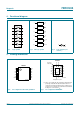
74HCU04 Nexperia Hex unbuffered inverter 4. Functional diagram $ < $ < $ < $ < $ < $ < PQD Fig 1. $ < PQD Logic symbol Fig 2. PQD IEC logic symbol Fig 3. Logic diagram (one inverter) 5.
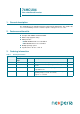
74HCU04 Nexperia Hex unbuffered inverter 5.1 Pin description Table 2. Pin description Symbol Pin Description 1A, 2A, 3A, 4A, 5A, 6A 1, 3, 5, 9, 11, 13 data input 1Y, 2Y, 3Y, 4Y, 5Y, 6Y 2, 4, 6, 8, 10, 12 data output GND 7 ground (0 V) VCC 14 supply voltage 6. Functional description Table 3. Function table H = HIGH voltage level; L = LOW voltage level Input Output nA nY L H H L 7. Limiting values Table 4.
74HCU04 Nexperia Hex unbuffered inverter 8. Recommended operating conditions Table 5. Recommended operating conditions Voltages are referenced to GND (ground = 0 V). Symbol Parameter VCC supply voltage Conditions Min Typ Max Unit 2.0 5.0 6.0 V VI input voltage 0 - VCC V VO output voltage 0 - VCC V Tamb ambient temperature 40 +25 +125 C 9. Static characteristics Table 6. Static characteristics Voltages are referenced to GND (ground = 0 V).
74HCU04 Nexperia Hex unbuffered inverter 10. Dynamic characteristics Table 7. Dynamic characteristics Voltages are referenced to GND (ground = 0 V); For test circuit see Figure 7. Symbol Parameter propagation delay tpd transition time tt power dissipation capacitance CPD [1] tpd is the same as tPHL, tPLH. [2] tt is the same as tTHL, tTLH. [3] 25 C Conditions 40 C to +85 C 40 C to Unit +125 C Typ Max Max Max VCC = 2.0 V; CL = 50 pF 19 70 90 105 ns VCC = 4.
74HCU04 Nexperia Hex unbuffered inverter 11. Waveforms 9, 90 Q$ LQSXW 90 *1' W 3+/ W 3/+ 92+ 9&& 38/6( *(1(5$725 90 90 Q< RXWSXW 92/ 9, 92 '87 &/ S) 57 W 7+/ W 7/+ PQD PQD VM = 0.5 VCC; VI = GND to VCC. Definitions for test circuit: CL = Load capacitance including jig and probe capacitance. RT = Termination resistance should be equal to output impedance Zo of the pulse generator. Fig 6. The input (nA) to output (nY) propagation delay times Fig 7.
4HCU04 Nexperia Hex unbuffered inverter DDO 92 9 ,' P$ 5ELDV Nȍ 9&& ) ) RXWSXW 9, I N+] LQSXW $ ,2 *1' 9, 9 PQD Tamb = 25 C. I g fs = --------OV I fi = 1 kHz at VO is constant Fig 10. VCC = 6.0 V; IO = 0 A Fig 11. Test set-up for measuring forward transconductance PQD J IV P$ 9 9&& 9 Tamb = 25 C. Fig 12.
74HCU04 Nexperia Hex unbuffered inverter 13. Application information Some applications are: • Linear amplifier (see Figure 13) • Crystal oscillator design (see Figure 14) • Astable multivibrator (see Figure 15) Remark: All values given are typical unless otherwise specified. 5 5 9&& ) 5 5 8 8 & =/ & RXW PQD PQD Maximum Vo(p-p) = VCC 2.0 V centered at 0.5 VCC.
74HCU04 Nexperia Hex unbuffered inverter Table 9. Optimum value for R2 Frequency R2 Optimum for 3 kHz 2.0 k minimum required ICC 8.0 k minimum influence due to change in VCC 6 kHz 1.0 k minimum required ICC 4.7 k minimum influence by VCC 0.5 k minimum required ICC 10 kHz 14 kHz >14 kHz 2.0 k minimum influence by VCC 0.5 k minimum required ICC 1.
74HCU04 Nexperia Hex unbuffered inverter 14.
74HCU04 Nexperia Hex unbuffered inverter 6623 SODVWLF VKULQN VPDOO RXWOLQH SDFNDJH OHDGV ERG\ ZLGWK PP ' 627 ( $ ; F \ + ( Y 0 $ = 4 $ $ $ $ SLQ LQGH[ ș / S / GHWDLO ; Z 0 E S H PP VFDOH ',0(16,216 PP DUH WKH RULJLQDO GLPHQVLRQV 81,7 $ PD[ $ $ $ E S F ' ( H + ( / / S 4 Y Z \ = ș PP
74HCU04 Nexperia Hex unbuffered inverter 76623 SODVWLF WKLQ VKULQN VPDOO RXWOLQH SDFNDJH OHDGV ERG\ ZLGWK PP ' 627 ( $ ; F \ + ( Y 0 $ = 4 $ SLQ LQGH[ $ $ $ ș / S / H GHWDLO ; Z 0 E S PP VFDOH ',0(16,216 PP DUH WKH RULJLQDO GLPHQVLRQV 81,7 $ PD[ $ $ $ E S F ' ( H + ( / / S 4 Y Z \ = ș PP
74HCU04 Nexperia Hex unbuffered inverter '+94)1 SODVWLF GXDO LQ OLQH FRPSDWLEOH WKHUPDO HQKDQFHG YHU\ WKLQ TXDG IODW SDFNDJH QR OHDGV WHUPLQDOV ERG\ [ [ PP % ' 627 $ $ $ ( F GHWDLO ; WHUPLQDO LQGH[ DUHD WHUPLQDO LQGH[ DUHD & H H Y Z E & $ % & \ \ & / (K H N 'K ; N PP VFDOH 'LPHQVLRQV PP DUH WKH RULJLQDO GLPHQVLRQV 8QLW PP PD[ QRP PLQ $ $ E F ' 'K ( (K H H
74HCU04 Nexperia Hex unbuffered inverter 15. Abbreviations Table 10. Abbreviations Acronym Description CMOS Complementary Metal Oxide Semiconductor LSTTL Low-power Schottky Transistor-Transistor Logic ESD ElectroStatic Discharge HBM Human Body Model MM Machine Model CDM Charge Device Model TTL Transistor-Transistor Logic 16. Revision history Table 11. Revision history Document ID Release date Data sheet status Change notice Supersedes 74HCU04 v.
74HCU04 Nexperia Hex unbuffered inverter 17. Legal information 17.1 Data sheet status Document status[1][2] Product status[3] Definition Objective [short] data sheet Development This document contains data from the objective specification for product development. Preliminary [short] data sheet Qualification This document contains data from the preliminary specification. Product [short] data sheet Production This document contains the product specification.
74HCU04 Nexperia Hex unbuffered inverter Export control — This document as well as the item(s) described herein may be subject to export control regulations. Export might require a prior authorization from competent authorities. Non-automotive qualified products — Unless this data sheet expressly states that this specific Nexperia product is automotive qualified, the product is not suitable for automotive use.
Nexperia 74HCU04 Hex unbuffered inverter 19. Contents 1 2 3 4 5 5.1 6 7 8 9 10 11 12 13 14 15 16 17 17.1 17.2 17.3 17.4 18 19 © General description . . . . . . . . . . . . . . . . . . . . . . 1 Features and benefits . . . . . . . . . . . . . . . . . . . . 1 Ordering information . . . . . . . . . . . . . . . . . . . . . 1 Functional diagram . . . . . . . . . . . . . . . . . . . . . . 2 Pinning information . . . . . . . . . . . . . . . . . . . . . . 2 Pin description . . . . . . . . . . . . . . . . . . .