
Data Sheet

©
Nexperia B.V. 2017. All rights reserved
BUK7620-100A All information provided in this document is subject to legal disclaimers.
Product data sheet Rev. 2 — 2 February 2011 3 of 13
Nexperia
BUK7620-100A
N-channel TrenchMOS standard level FET
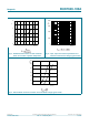
4. Limiting values
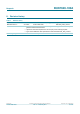
Table 4. Limiting values
In accordance with the Absolute Maximum Rating System (IEC 60134).
Symbol Parameter Conditions Min Max Unit
V
DS
drain-source voltage T
j
≥ 25 °C; T
j
≤ 175 °C - 100 V
V
DGR
drain-gate voltage R
GS
=20kΩ - 100 V
V
GS
gate-source voltage -20 20 V
I
D
drain current T
mb
=25°C; V
GS
=10V;
see Figure 1; see Figure 3
-63A
T
mb
=100°C; V
GS
= 10 V; see Figure 1 -44A
I
DM
peak drain current T
mb
= 25 °C; pulsed; t
p
≤ 10 µs;
see Figure 3
- 253 A
P
tot
total power dissipation T
mb
=25°C; see Figure 2 - 200 W
T
stg
storage temperature -55 175 °C
T
j
junction temperature -55 175 °C
Source-drain diode
I
S
source current T
mb
=25°C - 63 A
I
SM
peak source current pulsed; t
p
≤ 10 µs; T
mb
= 25 °C - 253 A
Avalanche ruggedness
E
DS(AL)S
non-repetitive drain-source
avalanche energy
I
D
=60A; V
sup
≤ 100 V; R
GS
=50Ω;
V
GS
=10V; T
j(init)
= 25 °C; unclamped
- 400 mJ
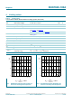
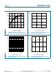
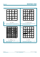
Fig 1. Normalized continuous drain current as a
function of mounting base temperature
Fig 2. Normalized total power dissipation as a
function of mounting base temperature
T
mb
(°C)
0 20015050 100
03aa24
40
80
120
I
der
(%)
0
T
mb
(°C)
0 20015050 100
03na19
40
80
120
P
der
(%)
0