
Data Sheet

©
Nexperia B.V. 2017. All rights reserved
BUK7620-100A All information provided in this document is subject to legal disclaimers.
Product data sheet Rev. 2 — 2 February 2011 5 of 13
Nexperia
BUK7620-100A
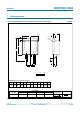
N-channel TrenchMOS standard level FET
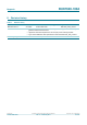
6. Characteristics
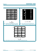
Table 6. Characteristics
Symbol Parameter Conditions Min Typ Max Unit
Static characteristics
V
(BR)DSS
drain-source
breakdown voltage
I
D
=0.25mA; V
GS
=0V; T
j
= 25 °C 100 - - V
I
D
=0.25mA; V
GS
=0V; T
j
= -55 °C 89 - - V
V
GS(th)
gate-source threshold
voltage
I
D
=1mA; V
DS
=V
GS
; T
j
=25°C;
see Figure 11
234V
I
D
=1mA; V
DS
=V
GS
; T
j
=-55°C;
see Figure 11
--4.4V
I
D
=1mA; V
DS
=V
GS
; T
j
= 175 °C;
see Figure 11
1--V
I
DSS
drain leakage current V
DS
=100V; V
GS
=0V; T
j
= 25 °C - 0.05 10 µA
V
DS
=100V; V
GS
=0V; T
j
= 175 °C - - 500 µA
I
GSS
gate leakage current V
GS
=20V; V
DS
=0V; T
j
= 25 °C - 2 100 nA
V
GS
=-20V; V
DS
=0V; T
j
= 25 °C - 2 100 nA
R
DSon
drain-source on-state
resistance
V
GS
=10V; I
D
=25A; T
j
= 175 °C;
see Figure 12; see Figure 13
--50mΩ
V
GS
=10V; I
D
=25A; T
j
=25°C;
see Figure 12
; see Figure 13
- 1720mΩ
Dynamic characteristics
C
iss
input capacitance V
GS
=0V; V
DS
=25V; f=1MHz;
T
j
=25°C; see Figure 14
- 3430 4373 pF
C
oss
output capacitance - 440 525 pF
C
rss
reverse transfer
capacitance
- 260 352 pF
t
d(on)
turn-on delay time V
DS
=30V; R
L
=1.2Ω; V
GS
=10V;
R
G(ext)
=10Ω; T
j
=25°C
-21-ns
t
r
rise time - 87 - ns
t
d(off)
turn-off delay time - 108 - ns
t
f
fall time - 56 - ns
L
D
internal drain
inductance
from upper edge of drain mounting base
to centre of die; T
j
=25°C
-2.5-nH
from drain lead 6 mm from package to
centre of die; T
j
=25°C
-4.5-nH
L
S
internal source
inductance
from source lead to source bond pad;
T
j
=25°C
-7.5-nH
Source-drain diode
V
SD
source-drain voltage I
S
=25A; V
GS
=0V; T
j
=25°C;
see Figure 15
- 0.85 1.2 V
t
rr
reverse recovery time I
S
=20A; dI
S
/dt = -100 A/µs;
V
GS
=-10V; V
DS
=30V; T
j
=25°C
-76-ns
Q
r
recovered charge - 282 - nC