Important notice Dear Customer, On 7 February 2017 the former NXP Standard Product business became a new company with the tradename Nexperia. Nexperia is an industry leading supplier of Discrete, Logic and PowerMOS semiconductors with its focus on the automotive, industrial, computing, consumer and wearable application markets In data sheets and application notes which still contain NXP or Philips Semiconductors references, use the references to Nexperia, as shown below. Instead of http://www.nxp.
SO T2 3 TL431 family Adjustable precision shunt regulator Rev. 5 — 01 September 2015 Product data sheet 1. Product profile 1.1 General description Three-terminal shunt regulator family with an output voltage range between Vref and 36 V, to be set by two external resistors. • The TL431xDBZR types feature an enhanced stability area with a very low load capacity requirement.
TL431 family NXP Semiconductors Adjustable precision shunt regulator 1.2 Features and benefits Programmable output voltage up to 36 V Three different reference voltage tolerances: Standard grade: 2 % A-Grade: 1 % B-Grade: 0.5 % Typical temperature drift: 6 mV (in a range of 0 C up to 70 C) Low output noise Typical output impedance: 0.2 Sink current capability: 1 mA to 100 mA AEC-Q100 qualified (grade 1) 1.
TL431 family NXP Semiconductors Adjustable precision shunt regulator 2. Pinning information Table 3.
TL431 family NXP Semiconductors Adjustable precision shunt regulator 3. Ordering information Table 4.
TL431 family NXP Semiconductors Adjustable precision shunt regulator 4. Marking Table 5.
TL431 family NXP Semiconductors Adjustable precision shunt regulator 6. Limiting values Table 6. Limiting values In accordance with the Absolute Maximum Rating System (IEC 60134). Symbol Parameter VKA Conditions Min Max Unit cathode-anode voltage - 37 V IK cathode current 100 150 mA Iref reference current 0.
TL431 family NXP Semiconductors Adjustable precision shunt regulator Table 7. ESD maximum ratings Tamb = 25 C unless otherwise specified. Symbol Parameter Conditions Min Max Unit VESD electrostatic discharge voltage MIL-STD-883 (human body model) - 4 kV 7. Recommended operating conditions Table 8. Operating conditions Symbol Parameter VKA IK Conditions Min Max Unit cathode-anode voltage Vref 36 V cathode current 1 100 mA 8. Thermal characteristics Table 9.
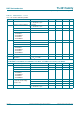
TL431 family NXP Semiconductors Adjustable precision shunt regulator 9. Characteristics Table 10. Characteristics Tamb = 25 C unless otherwise specified.
TL431 family NXP Semiconductors Adjustable precision shunt regulator Table 10. Characteristics …continued Tamb = 25 C unless otherwise specified. Symbol Parameter Conditions Min Typ Max Unit Iref reference current IK = 10 mA; R1 = 10 k; R2 = open - 2 4 A Iref reference current variation IK = 10 mA; R1 = 10 k; R2 = open IK(min) TL431ACDBZR Tamb = 0 C to 70 C - 0.4 1.2 A TL431AIDBZR Tamb = 40 C to 85 C - 0.8 2.
TL431 family NXP Semiconductors Adjustable precision shunt regulator Table 10. Characteristics …continued Tamb = 25 C unless otherwise specified. Symbol Parameter Conditions Iref reference current variation IK = 10 mA; R1 = 10 k; R2 = open IK(min) Min Typ Max Unit TL431BCDBZR Tamb = 0 C to 70 C - 0.4 1.2 A TL431BIDBZR Tamb = 40 C to 85 C - 0.8 2.5 A TL431BQDBZR TL431BFDT TL431BMFDT TL431BSDT TL431BMSDT Tamb = 40 C to 125 C - 0.4 0.
TL431 family NXP Semiconductors Adjustable precision shunt regulator 006aab571 2.60 IK (mA) Vref (V) 2.56 100 2.52 50 2.48 0 2.44 −50 2.40 −75 −25 25 75 −100 125 Tamb (°C) −2 −1 0 1 2 3 VKA (V) VKA = Vref; Tamb = 25 C IK = 10 mA; VKA = Vref Fig 3. 006aab572 150 Reference voltage as a function of ambient temperature; typical values Fig 4. Cathode current as a function of cathode-anode voltage; typical values INPUT VKA IK Vref GND 006aab573 IK = 10 mA; VKA = Vref Fig 5.
TL431 family NXP Semiconductors Adjustable precision shunt regulator 006aab574 5.0 006aab575 0 Iref (μA) ΔVref (mV) 4.0 −20 3.0 2.0 −40 1.0 0.0 −75 −25 25 75 −60 125 Tamb (°C) 10 20 30 40 VKA (V) IK = 10 mA; Tamb = 25 C IK = 10 mA; R1 = 10 k; R2 = open Fig 6. 0 Reference current as a function of ambient temperature; typical values Fig 7.
TL431 family NXP Semiconductors Adjustable precision shunt regulator 006aab577 250 Ioff (nA) 200 150 100 50 0 −75 −25 25 75 125 Tamb (°C) VKA = 36 V; Vref = 0 V Fig 9. Off-state current as a function of ambient temperature; typical values INPUT VKA Ioff GND 006aab578 VKA = 36 V; Vref = 0 V Fig 10. Off-state current as a function of ambient temperature; test circuit TL431 family Product data sheet All information provided in this document is subject to legal disclaimers. Rev.
TL431 family NXP Semiconductors Adjustable precision shunt regulator 006aab579 6 (1) Vin; Vout (V) 006aac478 6 (1) Vin; Vout (V) 4 4 (2) (2) 2 0 2 −1 0 1 3 5 7 t (μs) Tamb = 25 C −1 1 3 5 7 t (μs) Tamb = 25 C (1) Input (1) Input (2) Output (2) Output Fig 11. All types except TL431XFDT and TL431XSDT: Input voltage and output voltage as a function of time; typical values Fig 12.
TL431 family NXP Semiconductors Adjustable precision shunt regulator 006aab583 60 Av (dB) 006aac479 60 Av (dB) 40 40 20 20 0 1 10 102 103 104 0 102 10 1 103 f (kHz) 104 f (kHz) IK = 10 mA; Tamb = 25 C IK = 10 mA; Tamb = 25 C Fig 15. All types except TL431XFDT and TL431XSDT: Voltage amplification as a function of frequency; typical values Fig 16.
TL431 family NXP Semiconductors Adjustable precision shunt regulator 006aab585 102 ZKA (Ω) 006aac480 102 ZKA (Ω) 10 10 1 1 10−1 1 10 102 103 104 10−1 1 102 10 f (kHz) 103 104 f (kHz) IK = 10 mA; Tamb = 25 C IK = 10 mA; Tamb = 25 C Fig 19. All types except TL431XFDT and TL431XSDT: Dynamic cathode-anode impedance as a function of frequency; typical values Fig 20.
TL431 family NXP Semiconductors Adjustable precision shunt regulator 006aab588 100 IK (mA) 80 (1) (1) 60 Stable Oscillation Stable 40 20 0 1 102 10 103 104 CL (nF) Tamb = 25 C (1) VKA = Vref VKA = 5 V: no oscillation VKA = 10 V: no oscillation VKA = 15 V: no oscillation Fig 23. All types except TL431XFDT and TL431XSDT: Cathode current as a function of load capacitance; typical values 150 Ω IK R1 = 10 kΩ CL IK 150 Ω CL VBATT VBATT R2 GND VKA = Vref Tamb = 25 C Fig 24.
TL431 family NXP Semiconductors Adjustable precision shunt regulator 006aac481 100 IK (mA) 80 (1) (1) 60 Stable Oscillation Stable 40 20 0 10−1 1 10 102 103 104 CL (nF) Tamb = 25 C (1) VKA = Vref VKA = 5 V: no oscillation VKA = 10 V: no oscillation VKA = 15 V: no oscillation Fig 26.
TL431 family NXP Semiconductors Adjustable precision shunt regulator 006aab591 100 IK (mA) 80 (1) (1) (2) (2) 60 Stable Oscillation Stable 40 20 0 10−1 1 10 102 103 104 CL (nF) Tamb = 25 C (1) VKA = Vref (2) VKA = 5 V VKA = 10 V: no oscillation VKA = 15 V: no oscillation Fig 29.
TL431 family NXP Semiconductors Adjustable precision shunt regulator 10. Application information V+ VOUT R1 R2 006aab592 V OUT = 1 + R1 ------- V ref R2 Fig 32. Shunt regulator V+ VOUT R1 R2 006aab593 V OUT = 1 + R1 ------- V ref R2 V OUT min = V ref + V be Fig 33. Series pass regulator V+ VOUT VIN 006aab594 V th = V ref V IN V ref V OUT 0 V IN V ref V OUT 2V Fig 34.
TL431 family NXP Semiconductors Adjustable precision shunt regulator RCL V+ IOUT 006aab595 V ref I OUT = --------R CL Fig 35. Constant current source V+ VOUT R1 R2 006aab596 V OUT = 1 + R1 ------- V ref R2 Fig 36. High-current shunt regulator V+ ISINK RS 006aab597 V ref I SINK = --------RS Fig 37. Constant current sink TL431 family Product data sheet All information provided in this document is subject to legal disclaimers. Rev. 5 — 01 September 2015 © NXP Semiconductors N.V.
TL431 family NXP Semiconductors Adjustable precision shunt regulator REGULATOR LINE VOUT GND R3 R1 REF R2 GND 006aac482 Fig 38. TL431 in control loop of SMPS 11. Test information 11.1 Quality information This product has been qualified in accordance with the Automotive Electronics Council (AEC) standard Q100 - Failure mechanism based stress test qualification for integrated circuits, and is suitable for use in automotive applications. 12. Package outline 3.0 2.8 1.1 0.9 3 0.45 0.15 2.5 1.
TL431 family NXP Semiconductors Adjustable precision shunt regulator 13. Soldering 3.3 2.9 1.9 solder lands solder resist 3 2 1.7 solder paste 0.6 (3×) 0.7 (3×) occupied area Dimensions in mm 0.5 (3×) 0.6 (3×) 1 sot023_fr Fig 40. Reflow soldering footprint SOT23 (TO-236AB) 2.2 1.2 (2×) 1.4 (2×) solder lands 4.6 solder resist 2.6 occupied area Dimensions in mm 1.4 preferred transport direction during soldering 2.8 4.5 sot023_fw Fig 41.
TL431 family NXP Semiconductors Adjustable precision shunt regulator 14. Revision history Table 11. Revision history Document ID Release date Data sheet status Change notice Supersedes TL431_FAM v.5 20150901 Product data sheet - TL431_FAM v.4 Modifications: • Figure 18: Capacitor value corrected TL431_FAM v.4 20110630 Product data sheet - TL431_FAM v.3 TL431_FAM v.3 20101105 Product data sheet - TL431_FAM v.2 TL431_FAM v.2 20100120 Product data sheet - TL431_FAM v.
TL431 family NXP Semiconductors Adjustable precision shunt regulator 15. Legal information 15.1 Data sheet status Document status[1][2] Product status[3] Definition Objective [short] data sheet Development This document contains data from the objective specification for product development. Preliminary [short] data sheet Qualification This document contains data from the preliminary specification. Product [short] data sheet Production This document contains the product specification.
TL431 family NXP Semiconductors Adjustable precision shunt regulator No offer to sell or license — Nothing in this document may be interpreted or construed as an offer to sell products that is open for acceptance or the grant, conveyance or implication of any license under any copyrights, patents or other industrial or intellectual property rights. Translations — A non-English (translated) version of a document is for reference only.
NXP Semiconductors TL431 family Adjustable precision shunt regulator 17. Contents 1 1.1 1.2 1.3 1.4 2 3 4 5 6 7 8 9 10 11 11.1 12 13 14 15 15.1 15.2 15.3 15.4 16 17 Product profile . . . . . . . . . . . . . . . . . . . . . . . . . . 1 General description . . . . . . . . . . . . . . . . . . . . . 1 Features and benefits . . . . . . . . . . . . . . . . . . . . 2 Applications . . . . . . . . . . . . . . . . . . . . . . . . . . . 2 Quick reference data . . . . . . . . . . . . . . . . . . . .