
Users Manual

www.nicerf.com
LoRa1280/1F27
NiceRF Wireless Technology Co., Ltd. Rev 1.1
sales@nicerf.com
-6-
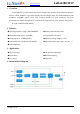
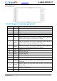
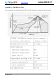
6. Pin definition
Note: All IO high level is 3.3V when powered by 5V
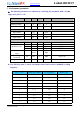
Pin NO. Pin name Description
1 VCC Positive power supply
2 GND Power ground
3 NRESET Chip reset trigger pin, active low
4 BUSY Status indicator foot (see SX1280/1281 specification for details)
5DIO1
Directly connected to the chip pin, configurable general-purpose IO
(see the c hip SX1280/1281 specification for details)
6DIO2
Directly connected to the chip pin, configurable general-purpose IO
(see the c hip SX1280/1281 specification for details)
7DIO3
Directly connected to the chip pin, configurable general-purpose IO
(see the c hip SX1280/1281 specification for details)
8 NSS Module chip select pin
9 SCK SPI clock input pin
10 MOSI SPI data input pin
11 MISO SPI data output pin
12,15.16 GND Connected to the negative pole
13 TXEN
Transmit control pin (high level when transmitting, low level when
receiving)
14 RXEN
Receive control pin (high level when receiving, low level when
transmitting)
17 ANT 50 ohm coaxial antenna
18 GND Can be connected to an ANT negative or left floating