
User Manual


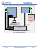


Table Of Contents

08-00040-01
VN400 Hardware Integration Application Note
Page 3/16
Proprietary & Confidential – NIVIS LLC
1. Purpose and Audience
The purpose of this document is to define the VN400 radio’s connectivity options and to provide the necessary data to
achieve hardware integration of the VN400 with a customer’s external application processor.
By definition, the VN400 is a radio module, approximately 1.0”W x 1.5”L, that is pre-loaded with the Nivis Smart Objects
communications stack. The small form factor enables the radio to be used in a variety of applications.
2. Pin-out and Interface Summary
The VN400 radio module uses the Freescale MC12311 SoC. Please refer to the block diagram in Figure 1 for the following
section.
The MC12311 operates in the 868 & 915 MHz ISM bands. It utilizes an internal PA (power amplifier) with a range of -20 to
+15 dBm at the antenna connector. The output power is adjustable in 1 dB steps.
The advantages of a radio module with adjustable power output are the following:
1. Ability to increase power output to +15 dBm for applications where battery consumption is not critical.
2. Enables the unit to be configured for different certification needs, especially locations that require reduced
power, such as Europe, Japan and China.
3. Provides greater power level consistency, for systems where symmetrical links are more critical.
The design of the RF section of the unit uses additional transmit components:
1. Dual LPF’s to reduce harmonic output and spurious output for regulatory compliance, such as FCC, IC, R&TTE,
and Giteki certifications.
2. Tx / Rx switch to select the transmit / receive RF path.
4. A SAW (Surface Acoustic Wave) filter is in line with the TX/RX path to significantly reduce out-of-band
interference as well as harmonic output.
As shown in the block diagram, the receive path utilizes the same Tx / Rx switch. The receive path is passive without any
additional amplification.
The Freescale SoC is clocked at 100MHz using a 15 ppm crystal, to maintain frequency stability. A 32.768 kHz real-time
clock IC is utilized to maintain SoC clocking operation during the low power / standby mode. An additional external flash
memory IC (serial) with a capacity of 2 MB is utilized for additional data storage. The Freescale Kinetis processor has the
ability to control MC12311 power and reset as needed for hibernate and low power modes.