
User Manual


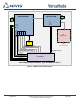


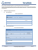

Table Of Contents

08-00040-01
VN400 Hardware Integration Application Note
Page 7/16
Proprietary & Confidential – NIVIS LLC
No.
Name
Description
Type
Dir
Comments
1
GND
Ground
N/A
N/A
2
Vin
Voltage Input 3.3V
N/A
I
3
GND
Ground
N/A
N/A
4
Vin
Voltage Input 3.3V
N/A
I
5
UART1_TXD
UART1 Transmit Data
DIG
O
Standard UART communication port.
6
UART1_RXD
UART1 Receive Data
DIG
I
Standard UART communication port.
7
nUART1_RTS
UART1 Request to Send
DIG
O
Standard UART communication port.
8
nUART1_CTS
UART1 Clear to Send
DIG
I
Standard UART communication port.
9
SPI1_SOUT
SPI Master Data Out
DIG
O
Standard SPI Communication port.
10
SPI1_SIN
SPI Master Data In
DIG
I
Standard SPI Communication port.
11
SPI1_SCK
SPI Clock Out
DIG
O
Standard SPI Communication port.
12
SPI_PCS0
SPI Slave Select
DIG
O
Standard SPI Communication port.
13
I2C_SDA
I2C Data Line
DIG
I/O
Standard I2C Communication
14
I2C_SCL
I2C Clock Line
DIG
O
Standard I2C Communication
15
RTC_OUT
RTC 1Hz Clock Out
DIG
O
See Notes (not available on current revision)
16
nRESET_K11
K11/K60 RESET pin
DIG
I
17
BOOT_SW
BOOT Switch
DIG
I
Switch to Firmware Load mode
BOOT_SW=”1” – normal operation
BOOT_SW=”0” – firmware update
18
LLWU_P13
Wake-Up Interrupt
DIG
O
19
3V3_OUT
Internal 3V3
N/A
O
Use for level shifting powering.
Low current output <20mA.
20
BKGD
BDM Background Mode
DIG
I/O
Standard BDM interface MC12311
21
JTAG_TMS
JTAG Test Mode Select
DIG
I
Standard JTAG interface Kinetis
22
nRESET_MC
MC12311 Reset pin
DIG
I
Standard BDM interface MC12311
23
JTAG_TDO
JTAG Test Data Output
DIG
O
Standard JTAG interface Kinetis
24
JTAG_TDI
JTAG Test Data Input
DIG
I
Standard JTAG interface Kinetis
25
PTA5
(JTAG_TRST)
UART/SPI App Mode
DIG
I
Define communication channel used by application
PTA5=”1” – UART Mode
PTA5=”0” – SPI Mode
26
JTAG_TCLK
JTAG Test Data Clock
DIG
I
Standard JTAG interface Kinetis
27
GND
Ground
N/A
N/A
28
GND
Ground
N/A
N/A
29
ADC_SE12
ADC pin SE12
Analog
I
12 bit Single Ended ADC,
Note: Analog Reference is Vdd=3.3V
30
ADC_SE13
ADC pin SE13
Analog
I
12 bit Single Ended ADC,
Note: Analog Reference is Vdd=3.3V
Table 1. Pin Definitions for VN400 Applications