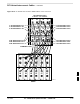
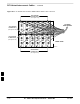
RF Cabinet Interconnect Cables – continued Figure H-14: SC 4812ET BTS Combiner DRDC/TRDC Cable Connection Dual Bandpass Filter 6 Sector – 1 or 2 Carrier 4B 1–1B 3064735A11 6 Sec 2–2B 3064735A07 6 Sec 3–3B 3064735A07 6 Sec 4A 1B 1A 5B 5A 2B 2A 6B 6A 3B 3A 1–1A 3064735A11 6 Sec 2–2A 3064735A07 6 Sec 3–3A 3064735A07 6 Sec 4–4B 3064735A12 6 Sec 5–5B 3064735A11 6 Sec 6–6B 3064735A07 6 Sec 4–4A 3064735A12 6 Sec 5–5A 3064735A11 6 Sec 6–6A 3064735A07 6 Sec COMBINER CAGE 3B 2B 1B 3A 6B 5B 4B
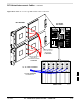
RF Cabinet Interconnect Cables – continued MPC Functional Description The MPC card provides (see Figure H-15) low-noise amplification for all RX path signals. The low noise, high gain design improves frame RX sensitivity and overcomes the splitting loss in the receive path. DC voltages are monitored on the RF devices and regulators and are used to generate hard and soft alarms. The MPC is not redundant at the card–level, but includes dual–path amplifiers which provide soft–fail redundancy for all sectors.
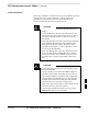
RF Cabinet Interconnect Cables – continued Figure H-15: DRDC To C–CCP Cage MPC Boards Cable Connections MPC BOARDS SC 4812ET RF Cabinet ETIB EBA RFDS 5 RU RACK SPACE CABLES CONNECT 1A, 2A, 3A TO TOP MPC BOARD # 3086659H01 CABLES CONNECT 1B, 2B, 3B TO BOTTOM MPC BOARD # 3086659H01 1A – 3A: CABLE # 3086659H01 1B – 3B: CABLE # 3086659H01 3B 2B 1B 3A 2A 1A * Use Cable 3086659H02 For Sectors 4 – 6 H DRDC CAGE Jan 2002 SC 4812ET BTS Optimization/ATP — CDMA LMF FW00710 H-21
RF Cabinet Interconnect Cables – continued RFDS Cabling Details Figure H-16 shows the components of the RFDS. Table H-2 depicts the cabling for a 3-Sector Duplexed configuration and Table H-3 depicts the cabling for a 6-Sector Duplexed configuration. Figure H-17 shows the connection of the RFDS to the BTS combiners.
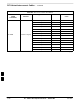
RF Cabinet Interconnect Cables – continued Table H-3: SC 4812ET Series 6-Sector Duplexed Directional Coupler to RFDS Cabling Table DRDC Label Directional Coupler Port Cobra RFDS Port ASU 1 – FWD (six pack MCX) 1A BTS Sector 1 Main BTS ASU1–FWD BTS–1 1B BTS Sector 1 Diversity BTS ASU1–FWD BTS–2 2A BTS Sector 2 Main BTS ASU1–FWD BTS–3 2B BTS Sector 2 Diversity BTS ASU1–FWD BTS–4 3A BTS Sector 3 Main BTS ASU1–FWD BTS–5 3B BTS Sector 3 Diversity BTS ASU1–FWD BTS–6 ASU 2 – FWD (six pack MCX
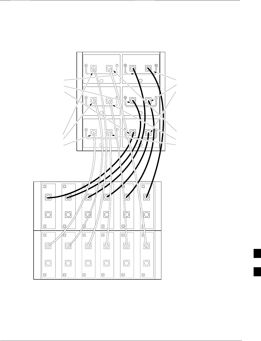
RF Cabinet Interconnect Cables – continued Figure H-17: SC 4812ET BTS Combiner DRDC/TRDC RFDS Cable Connection BTS COUPLED TO RFDS ASU 1 (See Figure H-16) ANT COUPLED TO RFDS ASU 1 (See Figure H-16) BTS COUPLED TO RFDS ASU 2 (See Figure H-16) 3B 2B 1B 3A 6B 5B 4B 6A 2A 5A TO RFDS ASU1 & ASU2 1A 4A DRDC CAGE FW00709 ANT COUPLED TO RFDS ASU 2 (See Figure H-16) H H-24 SC 4812ET BTS Optimization/ATP — CDMA LMF Jan 2002
RF Cabinet Interconnect Cables – continued 50 Pair Punchblock The 50 pair punchblock is the main interface point for RGPS, span lines, customer I/O, Power Cabinet alarm lines, and the modem. The punchblock provides primary protection for all lines. Refer to Figure H-18 and Table H-4 for punchblock pin–out.
RF Cabinet Interconnect Cables – continued Figure H-18: 50 Pair Punchblock TO MODEM CONNECTOR TO ALARMS CONNECTOR STRAIN RELIEVE INCOMING CABLE TO BRACKET WITH TIE WRAPS TO SPAN CONNECTOR RF Cabinet I/O Area TO RGD/RGPS CONNECTOR TOP VIEW OF PUNCH BLOCK 2R 2T LEGEND 1T = PAIR 1 – TIP 1R = PAIR 1 –RING ” ” ” ” ” ” 1R 1T SeeTable H-4 for Pin–Out.
RF Cabinet Interconnect Cables – continued Alarm and Span Line Cable Pin/Signal Information Table H-4 lists the complete pin/signal identification for the 50–pin punch block. Table H-4: Pin–Out for 50–Pair Punchblock Punchblock Cable Connector Signal Name Punch Pin Function Power Cabinet ALARM HSO/LFR Extension LFR Antenna Pilot Beacon Ext.
RF Cabinet Interconnect Cables – continued Table H-4: Pin–Out for 50–Pair Punchblock Punchblock Cable Connector ALARM Signal Name Punch Pin Function Customer Outputs Customer Outputs 1 – NO 14T Customer Outputs 1 – COM 14R Customer Outputs 1 – NO 14T Customer Outputs 1 – COM 14R Customer Outputs 1 – NC 15T Customer Outputs 2 – NO 15R Customer Outputs 2 – COM 16T Customer Outputs 2 – NC 16R Customer Outputs 3 – NO 17T Customer Outputs 3 – COM 17R Customer Outputs 3 – NC 18T Cust
RF Cabinet Interconnect Cables – continued Table H-4: Pin–Out for 50–Pair Punchblock Punchblock Cable Connector ALARM Signal Name Punch Pin Function Customer Inputs Customer Inputs 1 20T Cust_Rtn_A_1 20R Customer Inputs 2 21T Cust_Rtn_A_2 21R Customer Inputs 3 22T Cust_Rtn_A_3 22R Customer Inputs 4 23T Cust_Rtn_A_4 23R Customer Inputs 5 24T Cust_Rtn_A_5 24R Customer Inputs 6 25T Cust_Rtn_A_6 25R Customer Inputs 7 26T Cust_Rtn_A_7 26R Customer Inputs 8 27T Cust_Rtn_A_8 2
RF Cabinet Interconnect Cables – continued Table H-4: Pin–Out for 50–Pair Punchblock Punchblock Cable Connector Signal Name Punch Pin Function Span 1 Span 2 Span 3 SPAN I/O Span 4 Span 5 Span 6 RCV_TIP_A 30T RCV_RING_A 30R XMIT_TIP_A 31T XMIT_RING_A 31R RCV_TIP_B 32T RCV_RING_B 32R XMIT_TIP_B 33T XMIT_RING_B 33R RCV_TIP_C (Note) 34T RCV_RING_C (Note) 34R XMIT_TIP_C (Note) 35T XMIT_RING_C(Note) 35R RCV_TIP_D (Note) 36T RCV_RING_D (Note) 36R XMIT_TIP_D (Note) 37T XMIT
RF Cabinet Interconnect Cables – continued Table H-4: Pin–Out for 50–Pair Punchblock Punchblock Cable Connector Signal Name Punch Pin Function Ext.
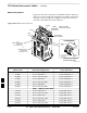
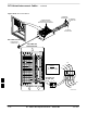
RF Cabinet Interconnect Cables – continued Figure H-19: SC 4812ET RF Cabinet Parts Locator 1 2 4 3 INDEX: 1. Door Switch 2. Door Switch (Main) 3. DC Power Distribution 4.
Appendix I: GPIB Addresses Appendix Content GPIB Addresses Introduction . . . . . . . . . . . . . . . . . . . . . . . . . . . . . . . . . . . . . . . . . . . . . . HP437 Power Meter GPIB Address . . . . . . . . . . . . . . . . . . . . . . . . . . . Gigatronics 8541C Power Meter GPIB Address . . . . . . . . . . . . . . . . . . Motorola CyberTest GPIB Address . . . . . . . . . . . . . . . . . . . . . . . . . . . . HP8935 Test Set GPIB Address . . . . . . . . . . . . . . . . . . . . . . . . . . . . . .
Table of Contents – continued Notes I SC 4812ET BTS Optimization/ATP — CDMA LMF Jan 2002
GPIB Addresses Introduction Use the procedures in this appendix to verify and/or change the GPIB addresses of the applicable test equipment. HP437 Power Meter GPIB Address Follow the steps in Table I-1 to verify and, if necessary, change the HP437 GPIB address. NOTE This procedure assumes that the test equipment is set up and ready for testing. Table I-1: Verify and/or Change HP437 Power Meter GPIB Address Step Action 1 Press Shift and PRESET (see Figure I-1).
GPIB Addresses – continued Gigatronics 8541C Power Meter GPIB Address Follow the steps in Table I-2 to verify and, if necessary, change the Gigatronics 8541C power meter GPIB address. NOTE This procedure assumes that the test equipment is set up and ready for testing. Table I-2: Verify and/or Change Gigatronics 8541C Power Meter GPIB Address Step Action ! CAUTION Do not connect/disconnect the power meter sensor cable with AC power applied to the meter.
GPIB Addresses – continued Motorola CyberTest GPIB Address Follow the steps in Table I-3 to verify and, if necessary, change the GPIB address on the Motorola CyberTest. Changing the GPIB address requires the following items: Motorola CyberTest communications analyzer Computer running Windows 3.1/Windows 95 Motorola CyberTAME software program “TAME” Parallel printer port cable (shipped with CyberTest) NOTE This procedure assumes that the test equipment is set up and ready for testing.
GPIB Addresses – continued HP8935 Test Set GPIB Address Follow the procedure in Table I-4 to verify and, if necessary, change the HP8935 GPIB address. NOTE This procedure assumes that the test equipment is set up and ready for testing. Table I-4: Verify and/or Change HP8935 GPIB Address Step Action * IMPORTANT The HP I/O configuration MUST be set to Talk & Listen, or NO device on the GPIB bus will be accessible. (Consult test equipment OEM documentation for additional information as required.
GPIB Addresses – continued Figure I-3: HP8935 Test Set Preset Local Inst Config Shift Cursor Control FW00885 I Jan 2002 SC 4812ET BTS Optimization/ATP — CDMA LMF I-5
GPIB Addresses – continued Setting HP8921A and HP83236A/B GPIB Address Follow the procedure in Table I-5 to verify and, if necessary, change the HP8921A HP83236A GPIB addresses. NOTE This procedure assumes that the test equipment is set up and ready for testing. Table I-5: Verify and/or Change HP8921A and HP83236A GPIB Addresses Step 1 Action To verify that the GPIB addresses are set correctly, press Shift and LOCAL on the HP8921A (see Figure I-4).
GPIB Addresses – continued Figure I-4: HP8921A and HP83236A/B Local Preset Shift Cursor Control I Jan 2002 SC 4812ET BTS Optimization/ATP — CDMA LMF I-7
GPIB Addresses – continued Advantest R3465 GPIB Address Table I-6 describes the steps to verify and, if necessary, change the GPIB address for the Advantest R3465. NOTE This procedure assumes that the test equipment is set up and ready for testing. Table I-6: Verify and/or Change Advantest R3465 GPIB Address Step Action 1 To verify that the GPIB address is set correctly, perform the following procedure: – Press SHIFT then PRESET (see Figure I-5). – Press LCL.
GPIB Addresses – continued RS232 GPIB Interface Box Ensure that the RS232 GPIB interface box dip switches are set as shown in Figure I-6.
CDMA 2000 Test Equipment Preparation Advantest R3267 Spectrum Analyzer GPIB Address Perform the procedure in Table I-7 and refer to Figure I-7 to verify and, if necessary, change the Advantest R3267 spectrum analyzer GPIB address. Table I-7: Verify and Change Advantest R3267 GPIB Address Step Action 1 If the REMOTE LED is lighted, press the LCL key. – The LED turns off. 2 Press the CONFIG key. – The CONFIG softkey labels will appear in the softkey label display area of the instrument display.
CDMA 2000 Test Equipment Preparation – continued Figure I-7: Setting Advantest R3267 GPIB Address Softkey Lable Display Area Softkey Buttons on REMOTE LED LCL Key CONFIG Key Keypad BS Key ENTR Key Advantest R3562 Signal Generator GPIB Address Set the GP–IB ADDRESS switch on the rear of the Advantest R3562 signal generator to address 1 as shown in Figure I-8.
CDMA 2000 Test Equipment Preparation – continued Agilent E4406A Transmitter Tester GPIB Address Follow the procedure in Table I-8 and refer to Figure I-9 to verify and, if necessary, change the Agilent E4406A GPIB address. Table I-8: Verify and Change Agilent E4406A GPIB Address Step Action 1 In the SYSTEM section of the instrument front panel, press the System key. – The softkey labels displayed on the right side of the instrument screen will change.
CDMA 2000 Test Equipment Preparation – continued Figure I-9: Setting Agilent E4406A GPIB Address Active Function Area Softkey Label Display Area Softkey Buttons System Key Data Entry Keypad Bk Sp Key Enter Key I Jan 2002 SC 4812ET BTS Optimization/ATP — CDMA LMF I-13
CDMA 2000 Test Equipment Preparation – continued Agilent E4432B Signal Generator GPIB Address Follow the procedure in Table I-9 and refer to Figure I-10 to verify and, if necessary, change the Agilent E4432B GPIB address. Table I-9: Verify and Change Agilent E4432B GPIB Address Step Action 1 In the MENUS section of the instrument front panel, press the Utility key. – The softkey labels displayed on the right side of the instrument screen will change.
CDMA 2000 Test Equipment Preparation – continued Figure I-10: Setting Agilent E4432B GPIB Address Active Entry Area Softkey Label Display Area Utility Key Softkey Buttons Numeric Keypad Backspace Key I Jan 2002 SC 4812ET BTS Optimization/ATP — CDMA LMF I-15
CDMA 2000 Test Equipment Preparation – continued Notes I I-16 SC 4812ET BTS Optimization/ATP — CDMA LMF Jan 2002
Appendix J: Download ROM Code Appendix Content Downloading ROM Code with the LMF . . . . . . . . . . . . . . . . . . . . . . . . . . . . . . Exception Procedure – Downloading ROM Code . . . . . . . . . . . . . . . . .
Table of Contents – continued Notes J SC 4812ET BTS Optimization/ATP — CDMA LMF Jan 2002
Downloading ROM Code with the LMF Exception Procedure – Downloading ROM Code This procedure is not part of a normal optimization. Perform this procedure only on an exception basis when no alternative exists to load a BTS device with the correct version of ROM code. NOTE One GLI must be INS_ACT (bright green) before ROM code can be downloaded to non–GLI devices. CAUTION The correct ROM and RAM codes for the software release used on the BSS must be loaded into BTS devices.
Downloading ROM Code with the LMF – continued CAUTION The Release level of the ROM code to be downloaded must be the one specified for the software release installed in the BSS. The release level of the ROM code resident in the other devices in the BTS must also be correct for the BSS software release being used. ROM code must not be downloaded to a frame loaded with code for a BSS software release with which it is not compatible. This procedure should only be used to upgrade replacement devices for a BTS.
Downloading ROM Code with the LMF – continued Table J-1: Download ROM and RAM Code to Devices Step Action ! CAUTION A ROM code file with the correct HW Bin Type must be chosen. Using a file with the wrong HW Bin Type can result in unpredictable operation and damage to the device. 9 10 Click on the ROM code file with the filename which matches the device type and HW Bin Type number noted in step 3 (for example, file bbx_rom.bin.0604 is the ROM code file for a BBX with a HW Bin Type of 0604).
Downloading ROM Code with the LMF – continued Notes J J-4 SC 4812ET BTS Optimization/ATP — CDMA LMF Jan 2002
K Appendix K: Optimizing Companion Frame Appendix Content Optimizing Companion Frame Optimizing the TX section of the Companion Frame – . . . . . . . . . . . . Optimizing the RX section of the Companion Frame – . . . . . . . . . . . .
K Table of Contents – continued Notes SC 4812ET BTS Optimization/ATP — CDMA LMF Jan 2002
Optimizing Companion Frame K Optimizing the TX section of the Companion Frame – The optimization/ATP procedure for the transmit side of the Companion Frame is identical to that of the SC4812ET BTS. Table K-1: Optimizing the TX section of the Companion Frame Step Action 1 Please refer to the TX Optimization/ATP – Chapter 3 of this manual for step–by–step TX Optimization/ATP instructions for the standalone frame 2 Run the TX tests.
K Optimizing Companion Frame – continued Optimizing the RX section of the Companion Frame – RX (Main) Optimization/ATP To test the RX Main antenna system follow the instructions in Table K-2 and refer to illustration Figure K-1(3–sector configuration). Table K-2: Optimizing the RX (Main) section of the Companion Frame Step Action 1 Connect the RX test cables to the antenna ports 1A–3A (for 3–sector optimization) or antenna ports 1A–6A (for 6–sector optimization).
Optimizing Companion Frame – continued K Figure K-2: WinLMF Display Screen Jan 2002 SC 4812ET BTS Optimization/ATP — CDMA LMF K-3
K Optimizing Companion Frame – continued Notes K-4 SC 4812ET BTS Optimization/ATP — CDMA LMF Jan 2002
Index Numbers test matrix/detailed optimization, B-1 10BaseT/10Base2 Converter, 1-7 ATP – Code Domain Power, 4-11 2–way Splitter, 1-11 ATP – Frame Error Rate (FER), 4-13 3–Sector Duplexed Directional Coupler to RFDS Cabling Table, H-22 ATP – Pilot Time Offset, 4-10 ATP – Reduced, 4-2 4812ET RF Cabinet Internal FRU Locations, H-3 ATP – Spectral Purity Transmit Mask, 4-7 6–Sector Duplexed Directional Coupler to RFDS Cabling Table, H-23 ATP – Waveform Quality (rho), 4-9 ATP Report, 4-14 ATP Test Pr
Index – continued cable calibration, automatic, test set–up, 3-50, 3-51 Advantest R3267/R3562, 3-51 Advantest R3465, 3-50 Agilent 8935, 3-50 Agilent E4406A/E4432B, 3-51 CyberTest, 3-50 HP 8921A, 3-50 cdpower test, 4-11 Cables Connection for 10 MHz Signal and GPIB , F-2, F-4 Channel Service Unit, 3-4 Calibrate BLO, 3-73 CIO Connectors, 6-14 Calibrating Cables, 3-67 CLI, 1-2 Calibrating Test Cable Setup, PCS Interface HP83236B, F-11 Clock Sync Module.
Index – continued Detailed, optimization/ATP test matrix, B-1 Gigatronics 8542B power meter, illustration, I-2 Devices, download. See Download Gigatronics Power Meter, 3-46 Digital Control Problems, 6-15 C–CCP Backplane Troubleshooting, 6-15 GLI.
Index – continued HSO Initialization/Verification, 3-35 LPAC Interface Board, H-11 I M I and Q values, E-1 major components, 1-17 In–Service Calibration, G-15 test set–up diagrams DRDC, Advantest, 3-58 TRDC, Advantest, 3-60 Manual, layout, 1-1 Master Group Line Interface.
Index – continued Optimization, 1-1 optimization/ATP, test set–up, 3-55 Advantest R3267/R3562 DRDCs, 3-58 TRDCs, 3-60 Advantest R3465, 3-55 Agilent 8935 DRDCs, 3-57 TRDCs, 3-59 Agilent E4406A/E4432B DRDCs, 3-57 TRDCs, 3-59 CyberTest, 3-55 HP 8921A, 800 MHz, 3-56 HP 8921A, 1.
Index – continued RF Adapters, 1-10 Setting Control Port, 3-5 RF Attenuators, 1-9 Setting Coupler Loss Value, 3-72 50 Pair Punchblock, H-25 SGLI2, board detail, MMI port connections, 5-4 RF Path Bay Level Offset Calibration, 3-73 SIF, output considerations vs BBX gain set point, C-1 RF Test Cable, 1-10 Site, equipage verification, 3-3 RFDS – Fault Isolation, 6-20 Site checklist, verification data sheets, A-2 RFDS Cabling Details, H-22 site equippage, CDF file, 3-2 RFDS calibration descriptio
Index – continued Test equipment connections , F-1 preliminary Agilent E4406A/E4432B set–up, F-10 Test Equipment Policy, 1-4 Test Equipment Setup, 3-45 Test Equipment Setup Calibration for TX Bay Level Offset, 3-70, F-15 Test Equipment Setup Chart, 3-47 Test equipment setup RF path calibration, 3-77 Test Set Calibration, 3-63 Advantest R3465, 3-53 Agilent 8935, 3-52 Agilent E4406A, 3-54 CyberTest, 3-52 HP 8921A, 3-53 TX Code Domain Power ATP, 4-11 tx fine adjust, E-1 TX Mask Verification, spectrum analyz
Index – continued Notes Index-8 SC 4812ET BTS Optimization/ATP — CDMA LMF Jan 2002