Prepare to Leave the Site External Test Equipment Removal Perform the procedure in Table 5-1 to disconnect the test equipment and configure the BTS for active service. Table 5-1: External Test Equipment Removal Step Action 1 Disconnect all external test equipment from all TX and RX connectors at the rear of the frame. 2 Reconnect and visually inspect all TX and RX antenna feed lines at the rear of the frame. CAUTION Verify all sector antenna feed lines are connected to the correct ports on the frame.
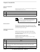
Prepare to Leave the Site – continued Table 5-2: Copy Files from LMF to a Diskette Step Action 3 Click on your C: drive. 4 Double Click on the wlmf folder. 5 Double Click on the CDMA folder. 6 Click on the bts–# folder for the calibration file you want to copy. 7 Drag the BTS–#.cal file to the 3–1/2 floppy (A:) icon on the top left of the screen and release the mouse button.
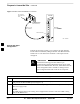
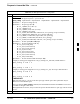
Prepare to Leave the Site – continued BTS Site Span Configuration Verification Perform the procedure in Table 5-4 to verify the current Span Framing Format and Line Build Out (LBO) parameters. ALL MGLI2/SGLI2 boards in all C–CCP shelves that terminate a T1/E1 span should be verified. Table 5-4: BTS Span Parameter Configuration Step Action 1 Connect a serial cable from the LMF COM1 port (via null modem board) to the front panel of the MGLI2 MMI port (see Figure 5-1).
Prepare to Leave the Site – continued Figure 5-1: MGLI2/SGLI2 MMI Port Connection RS–232 CABLE FROM LMF COM1 PORT GLI BOARD NULL MODEM BOARD (PART# 8484877P01) 9–PIN TO 9– PIN RS–232 CABLE MMI SERIAL PORT REF– FW00344 5 Set BTS Site Span Configuration Perform the procedure in Table 5-5 to configure the Span Framing Format and Line Build Out (LBO) parameters. ALL MGLI2/SGLI2 boards in all C–CCP shelves that terminate a T1/E1 span must be configured.
Prepare to Leave the Site – continued Table 5-5: Set BTS Span Parameter Configuration Step Action 3 If required only, enter the following MMI command for each span line to set the BTS span parameters to match that of the physical spans a – f run to the site: span_config option#1 = the span to change (a – f) option#2 = the span type (0 – 8): 0 – E1_1 (HDB3, CCS, CRC–4) 1 – E1_2 (HDB3, CCS) 2 – E1_3 (HDB3, CAS, CRC–4, TS16) 3 – E1_4 (HDB3, CAS, TS16)
Prepare to Leave the Site – continued Table 5-5: Set BTS Span Parameter Configuration Step Action 5 This completes the site specific BTS Span setup for this GLI. Move the MMI cable to the next SGLI2 and repeat steps 1 and 4 for ALL MGLI2/SGLI2 boards. 6 Terminate the Hyperterm session and disconnect the LMF from the MGLI/SGLI. Re–connect BTS T1 Spans and Integrated Frame Modem Before leaving the site, connect any T1 span TELCO connectors which were removed to allow the LMF to control the BTS.
Prepare to Leave the Site – continued Reestablish OMC-R Control/ Verifying T1/E1 IMPORTANT * After all activities at the site have been completed, including disconnecting the LMF, place a phone call to the OMC-R and request the BTS be placed under control of the OMC-R.
Prepare to Leave the Site – continued Notes 5 5-8 SC 4812ET BTS Optimization/ATP — CDMA LMF Jan 2002
Chapter 6: Basic Troubleshooting Table of Contents Jan 2002 Basic Troubleshooting Overview Overview . . . . . . . . . . . . . . . . . . . . . . . . . . . . . . . . . . . . . . . . . . . . . . . . 6-1 Troubleshooting: Installation Cannot Log into Cell-Site . . . . . . . . . . . . . . . . . . . . . . . . . . . . . . . . . . . Cannot Communicate to Power Meter . . . . . . . . . . . . . . . . . . . . . . . . . Cannot Communicate to Communications Analyzer . . . . . . . . . . . . . .
Table of Contents – continued DC Power Problems . . . . . . . . . . . . . . . . . . . . . . . . . . . . . . . . . . . . . . . TX and RX Signal Routing Problems . . . . . . . . . . . . . . . . . . . . . . . . . . 6-17 6-19 RFDS – Fault Isolation Introduction . . . . . . . . . . . . . . . . . . . . . . . . . . . . . . . . . . . . . . . . . . . . . . All tests fail . . . . . . . . . . . . . . . . . . . . . . . . . . . . . . . . . . . . . . . . . . . . . . All RX and TX paths fail . . . . . . . . . . . . .
Basic Troubleshooting Overview Overview The information in this chapter addresses some of the scenarios likely to be encountered by Customer Field Engineering (CFE) team members. This troubleshooting guide was created as an interim reference document for use in the field. It provides basic “what to do if” basic troubleshooting suggestions when the BTS equipment does not perform per the procedure documented in the manual.
Troubleshooting: Installation Cannot Log into Cell-Site Follow the procedure in Table 6-1 to troubleshoot any Login Failure problem during normal operation. Table 6-1: Login Failure Troubleshooting Procedure 6 Step Action 1 If MGLI2 LED is solid RED, it implies a hardware failure. Reset MGLI2 by re-seating it. If this persists, install RGLI2 card in MGLI2 slot and retry. A Red LED may also indicate no Ethernet termination at top of frame.
Troubleshooting: Installation – continued Cannot Communicate to Communications Analyzer Follow the procedure in Table 6-3 to troubleshoot a communication analyzer failure. Table 6-3: Troubleshooting a Communications Analyzer Communication Failure Step Action 1 Verify analyzer is connected to LMF with GPIB adapter. 2 Verify cable setup. 3 Verify the GPIB address is set to 18. 4 Verify the GPIB adapter DIP switch settings are correct. Refer to Test Equipment setup section for details.
Troubleshooting: Download Code Download Failure Follow the procedure in Table 6-4 to troubleshoot any code download failure. Table 6-4: Troubleshooting Code Download Failure Step Action 1 Verify T1 is disconnected from the BTS at CSU. 2 Verify LMF can communicate with the BTS device using the Status function. 3 Communication to MGLI2 must first be established before trying to talk to any other BTS device. MGLI2 must be INS_ACT state (green).
Troubleshooting: Download – continued Cannot ENABLE Device Before a device can be enabled (placed in-service), it must be in the OOS_RAM state (yellow on the LMF) with data downloaded to the device. The color of the device on the LMF changes to green, once it is enabled. The three states that devices can be displayed: Enabled (green, INS) Disabled (yellow, OOS_RAM) Reset (blue, OOS_ROM) Follow the procedure in Table 6-6 to troubleshoot device enable failure.
Troubleshooting: Calibration Bay Level Offset Calibration Failure Follow the procedure in Table 6-8 to troubleshoot a BLO calibration failure. Table 6-8: Troubleshooting BLO Calibration Failure 6 6-6 Step Action 1 Verify the Power Meter is configured correctly (see the test equipment setup section) and connection is made to the proper TX port. 2 Verify the parameters in the bts–#.
Troubleshooting: Calibration – continued Calibration Audit Failure Follow the procedure in Table 6-9 to troubleshoot a calibration audit failure. Table 6-9: Troubleshooting Calibration Audit Failure Step Action 1 Verify Power Meter is configured correctly (refer to the test equipment setup section of chapter 3). 2 Re-calibrate the Power Meter and verify it is calibrated correctly with cal factors from sensor head. 3 Verify that no LPA is in alarm state (rapidly flashing red LED).
Troubleshooting: Transmit ATP Forward link problem If the BTS passes the reduced ATP tests but has a forward link problem during normal operation follow the procedure in Table 6-10 to troubleshoot.
Troubleshooting: Transmit ATP – continued Table 6-12: Troubleshooting Rho and Pilot Time Offset Measurement Failure Step Action 5 Verify that no LPA in the sector is in alarm state (flashing red LED). Reset the LPA by pulling the circuit breaker, and, after 5 seconds, pushing back in. 6 If Rho value is unstable and varies considerably (e.g. .95,.92,.93), this may indicate that the GPS is still phasing (i.e. trying to reach and maintain 0 freq. error). Go to the freq.
Troubleshooting: Receive ATP Multi–FER Test Failure Follow the procedure in Table 6-15 to troubleshoot multi–FER failure. Table 6-15: Troubleshooting Multi-FER Failure Step Action 1 Verify test equipment set up is correct for a FER test. 2 Verify test equipment is locked to 19.6608 and even second clocks. The yellow LED (REF UNLOCK) must be OFF. 3 Verify MCCs have been loaded with data and are INS–ACT. 4 Disable and re-enable the MCC (one or more based on extent of failure).
Troubleshooting: CSM Checklist Problem Description Many of the Clock Synchronization Manager (CSM) boards may be resolved in the field before sending the boards to the factory for repair. This section describes known CSM problems identified in field returns, some of which are field-repairable. Check these problems before returning suspect CSM boards. Intermittent 19.
Troubleshooting: CSM Checklist – continued CSM Reference Source Configuration Error This is caused by incorrect reference source configuration performed in the field by software download. CSM kit SGLN1145 and SGLN4132 must have proper reference sources configured (as shown below) to function correctly. CSM Kit No. SGLN1145 SGLN4132ED or later Hardware Configuration CSM Slot No.
C–CCP Backplane Troubleshooting Introduction The C–CCP backplane is a multi–layer board that interconnects all the C–CCP modules. The complexity of this board lends itself to possible improper diagnoses when problems occur. Connector Functionality The following connector overview describes the major types of backplane connectors along with the functionality of each. This will allow the Cellular Field Engineer (CFE) to: Determine which connector(s) is associated with a specific problem type.
CCP Backplane Troubleshooting – continued GLI2 Ethernet “A” and “B” Connections These BNC connectors are located on the C–CCP backplane and routed to the GLI2 board. This interface provides all the control and data communications between the master GLI2 and the other GLI2, between gateways, and for the LMF on the LAN. BBX2 Connector Each BBX connector consists of a Harting 2SU/1SU digital connector and two 6–conductor coaxial connectors.
CCP Backplane Troubleshooting – continued Digital Control Problems No GLI2 Control via LMF (all GLI2s) Follow the procedure in Table 6-16 for problems with GLI2 control. Table 6-16: No GLI2 Control via LMF (all GLI2s) Step Action 1 Check the ethernet for proper connection, damage, shorts, or opens. 2 Verify C–CCP backplane Shelf ID DIP switch is set correctly. 3 Visually check the master GLI2 connector (both board and backplane) for damage. 4 Replace the master GLI2 with a known good GLI2.
CCP Backplane Troubleshooting – continued No AMR Control (MGLI2 good) Follow the procedure in Table 6-19 for problems with AMR control. Table 6-19: MGLI2 Control Good – No Control over AMR Step Action 1 Visually check the master GLI2 connector (both board and backplane) for damage. 2 Replace the master GLI2 with a known good GLI2. 3 Replace the AMR with a known good AMR. No BBX Control in the Shelf Follow the procedure in Table 6-20 for problems with co–located GLI2.
CCP Backplane Troubleshooting – continued No (or Missing) MCC24 Channel Elements Follow the procedure in Table 6-22 for problems with channel elements. Table 6-22: No MCC–1X/MCC24E/MCC8E Channel Elements Step Action 1 Verify channel elements on a co–located MCC of the same MCC8E = 0; MCC24E = 2; MCC–1X = 3) type (CDF MccType codes: 2 Check MCC connectors (both module and backplane) for damage. 3 If the problem seems to be limited to one MCC, replace it with a known good MCC of the same type.
CCP Backplane Troubleshooting – continued No DC Input Voltage to Power Supply Module Follow the procedure in Table 6-23 for problems with DC input voltage. Table 6-23: No DC Input Voltage to Power Supply Module Step 1 Action Verify DC power is applied to the BTS frame. Verify there are no breakers tripped. * IMPORTANT If a breaker has tripped, remove all modules from the applicable shelf supplied by the breaker and attempt to reset it.
CCP Backplane Troubleshooting – continued No DC Voltage (+5, +6.5, or +15 Volts) to a Specific GLI2, BBX2, or Switchboard Follow the procedure in Table 6-24 for problems with DC input voltage. Table 6-24: No DC Input Voltage to any C–CCP Shelf Module Step Action 1 Verify steps outlined in Table 6-23 have been performed. 2 Inspect the defective board/module (both board and backplane) connector for damage. 3 Replace suspect board/module with known good board/module.
RFDS – Fault Isolation Introduction The RFDS is used to perform Pre–Calibration Verification and Post-Calibration Audits which limit-check the RFDS-generate and reported receive levels of every path from the RFDS through the directional coupler coupled paths. In the event of test failure, refer to the following tables. All tests fail Follow the procedure in Table 6-26 for problems with RFDS.
RFDS – Fault Isolation – continued All tests fail on a single antenna If all path failures are on one antenna port, forward and/or reflected, follow the procedures in Table 6-28 checks. Table 6-28: RFDS Fault Isolation – All tests fail on single antenna path Step Action 1 Visually inspect the site interface cabinet internal cabling to the suspect directional coupler antenna port. 2 Verify the forward and reflected ports connect to the correct RFDS antenna select unit positions on the RFDS backplane.
Module Front Panel LED Indicators and Connectors Module Status Indicators Each of the non-passive plug-in modules has a bi-color (green & red) LED status indicator located on the module front panel. The indicator is labeled PWR/ALM. If both colors are turned on, the indicator is yellow. Each plug-in module, except for the fan module, has its own alarm (fault) detection circuitry that controls the state of the PWR/ALM LED. The fan TACH signal of each fan module is monitored by the AMR.
Module Front Panel LED Indicators and Connectors – continued CSM LED Status Combinations PWR/ALM LED The CSMs include on-board alarm detection. Hardware and software/firmware alarms are indicated via the front panel indicators. After the memory tests, the CSM loads OOS–RAM code from the Flash EPROM, if available. If not available, the OOS–ROM code is loaded from the Flash EPROM. Solid GREEN – module is INS_ACT or INS_STBY no alarm.
Module Front Panel LED Indicators and Connectors – continued FREQ Monitor Connector A test port provided at the CSM front panel via a BNC receptacle allows monitoring of the 19.6608 MHz clock generated by the CSM. When both CSM 1 and CSM 2 are in an in-service (INS) condition, the CSM 2 clock signal frequency is the same as that output by CSM 1. The clock is a sine wave signal with a minimum amplitude of +2 dBm (800 mVpp) into a 50 Ω load connected to this port.
Module Front Panel LED Indicators and Connectors – continued GLI2 LED Status Combinations The GLI2 module has indicators, controls and connectors as described below and shown in Figure 6-2. The indicators and controls consist of: Four LEDs One pushbutton ACTIVE LED Solid GREEN – GLI2 is active. This means that the GLI2 has shelf control and is providing control of the digital interfaces. Off – GLI2 is not active (i.e., Standby). The mate GLI2 should be active.
Module Front Panel LED Indicators and Connectors – continued GLI2 Pushbuttons and Connectors RESET Pushbutton – Depressing the RESET pushbutton causes a partial reset of the CPU and a reset of all board devices. GLI2 will be placed in the OOS_ROM state MMI Connector – The RS–232MMI port connector is intended to be used primarily in the development or factory environment but may be used in the field for debug/maintenance purposes.
Module Front Panel LED Indicators and Connectors – continued BBX LED Status Combinations PWR/ALM LED The BBX module has its own alarm (fault) detection circuitry that controls the state of the PWR/ALM LED.
Module Front Panel LED Indicators and Connectors – continued Figure 6-3: MCC24/8E Front Panel LEDs and LED Indicators PWR/ALM PWR/ALM LED LED COLOR OFF − operating normally ON − briefly during power up and during failure ;conditions An alarm is generated in the event of a failure PWR/ALM LENS (REMOVABLE) ACTIVE RED GREEN RED ACTIVE ACTIVE LED OPERATING STATUS RAPIDLY BLINKING − Card is code loaded but ;not enabled SLOW BLINKING − Card is not code loaded ON − card is code loaded and enabled ;(
Basic Troubleshooting – Span Control Link Span Problems (No Control Link) Follow the procedure in Table 6-29 when troubleshooting a control link failure. Table 6-29: Troubleshooting Control Link Failure Step 1 Action Verify the span settings using the span_view command on the active master GLI2 MMI port. If these are set correctly, verify the edlc parameters using the show command. Any alarms conditions indicate that the span is not operating correctly.
Basic Troubleshooting – Span Control Link – continued Notes 6 6-30 SC 4812ET BTS Optimization/ATP — CDMA LMF Jan 2002
A Appendix A: Data Sheets Appendix Content Appendix A: Optimization (Pre–ATP) Data Sheets Verification of Test Equipment Used . . . . . . . . . . . . . . . . . . . . . . . . . . . Site Checklist . . . . . . . . . . . . . . . . . . . . . . . . . . . . . . . . . . . . . . . . . . . . . Preliminary Operations . . . . . . . . . . . . . . . . . . . . . . . . . . . . . . . . . . . . . Pre–Power and Initial Power Tests . . . . . . . . . . . . . . . . . . . . . . . . . . . . General Optimization Checklist . . . .
A Table of Contents – continued Notes SC 4812ET BTS Optimization/ATP — CDMA LMF Jan 2002
Appendix A: Optimization (Pre–ATP) Data Sheets A Verification of Test Equipment Used Table A-1: Verification of Test Equipment Used Manufacturer Model Serial Number Comments:________________________________________________________ __________________________________________________________________ Jan 2002 SC 4812ET BTS Optimization/ATP — CDMA LMF A-1
A Appendix A: Optimization (Pre–ATP) Data Sheets – continued Site Checklist Table A-2: Site Checklist OK Parameter Specification Deliveries Per established procedures Floor Plan Verified Inter Frame Cables: Ethernet Frame Ground Power Per procedure Per procedure Per procedure Factory Data: BBX Test Panel RFDS Per procedure Per procedure Per procedure Site Temperature Dress Covers/Brackets Comments Preliminary Operations Table A-3: Preliminary Operations OK Paramete
Appendix A: Optimization (Pre–ATP) Data Sheets – continued A Pre–Power and Initial Power Tests Table A3a: Pre–power Checklist OK Parameter Pre–power–up tests Specification Verify power supply output voltage at the top of each BTS frame is within specifications Internal Cables: ISB (all cages) CSM (all cages) Power (all cages) Ethernet Connectors LAN A ohms LAN B ohms LAN A shield LAN B shield Ethernet Boots Air Impedance Cage (single cage) installed Initial power–up tests Verify
A Appendix A: Optimization (Pre–ATP) Data Sheets – continued General Optimization Checklist Table A3b: Pre–power Checklist OK Parameter Specification LEDs Frame fans illuminated operational LMF to BTS Connection Preparing the LMF Log into the LMF PC Create site specific BTS directory Download device loads per procedure per procedure per procedure per procedure Ping LAN A Ping LAN B per procedure per procedure Download/Enable MGLI2s Download/Enable GLI2s Set S
Appendix A: Optimization (Pre–ATP) Data Sheets – continued A GPS Receiver Operation Table A-4: GPS Receiver Operation OK Parameter Specification GPS Receiver Control Task State: tracking satellites Verify parameter Initial Position Accuracy: Verify Estimated or Surveyed Current Position: lat lon height RECORD in msec and cm also convert to deg min sec Current Position: satellites tracked Estimated: (>4) satellites tracked,(>4) satellites visible Surveyed: (>1) satellite tracked,(>4) s
A Appendix A: Optimization (Pre–ATP) Data Sheets – continued LFR Receiver Operation Table A-5: LFR Receiver Operation OK Parameter Specification Station call letters M X Y Z assignment.
Appendix A: Optimization (Pre–ATP) Data Sheets – continued A LPA IM Reduction Table A-6: LPA IM Reduction Parameter OK Comments CARRIER LPA # Specification 4:1 & 2:1 3–Sector 2:1 6–Sector Dual BP 3–Sector Dual BP 6–Sector 1A C1 C1 C1 C1 No Alarms 1B C1 C1 C1 C1 No Alarms 1C C1 C1 C1 C1 No Alarms 1D C1 C1 C1 C1 No Alarms 2A C2 C2 C2 No Alarms 2B C2 C2 C2 No Alarms 2C C2 C2 C2 No Alarms 2D C2 C2 C2 No Alarms 3A C3 C1 C1 No Al
A Appendix A: Optimization (Pre–ATP) Data Sheets – continued TX Bay Level Offset / Power Output Verification for 3–Sector Configurations 1–Carrier 2–Carrier Non–adjacent Channels 4–Carrier Non–adjacent Channels Table A-7: TX BLO Calibration (3–Sector: 1–Carrier, 2–Carrier and 4–Carrier Non–adjacent Channels) OK Parameter Specification Comments BBX–1, ANT–1 = BBX–r, ANT–1 = dB dB BBX–2, ANT–2 = BBX–r, ANT–2 = dB dB BBX–3, ANT–3 = BBX–r, ANT–3 = dB dB BBX–7, ANT–1 = BBX–r, ANT–1 = dB dB BBX
Appendix A: Optimization (Pre–ATP) Data Sheets – continued A Table A-7: TX BLO Calibration (3–Sector: 1–Carrier, 2–Carrier and 4–Carrier Non–adjacent Channels) OK Parameter Specification Comments BBX–1, ANT–1 = BBX–r, ANT–1 = dB dB BBX–2, ANT–2 = BBX–r, ANT–2 = dB dB BBX–3, ANT–3 = BBX–r, ANT–3 = dB dB BBX–7, ANT–1 = BBX–r, ANT–1 = dB dB BBX–8, ANT–2 = BBX–r, ANT–2 = dB dB BBX–9, ANT–3 = BBX–r, ANT–3 = dB dB BBX–4, ANT–1 = BBX–r, ANT–1 = dB dB BBX–5, ANT–2 = BBX–r, ANT–2 = dB
A Appendix A: Optimization (Pre–ATP) Data Sheets – continued 2–Carrier Adjacent Channel Table A-8: TX Bay Level Offset Calibration (3–Sector: 2–Carrier Adjacent Channels) OK Parameter Specification Comments BBX–1, ANT–1 = BBX–r, ANT–1 = dB dB BBX–2, ANT–2 = BBX–r, ANT–2 = dB dB BBX–3, ANT–3 = BBX–r, ANT–3 = dB dB BBX–7, ANT–4 = BBX–r, ANT–4 = dB dB BBX–8, ANT–5 = BBX–r, ANT–5 = dB dB BBX–9, ANT–6 = BBX–r, ANT–6 = dB dB BBX–1, ANT–1 = BBX–r, ANT–1 = dB dB BBX–2, ANT–2 = BBX–r,
Appendix A: Optimization (Pre–ATP) Data Sheets – continued A 3–Carrier Adjacent Channels 4–Carrier Adjacent Channels Table A-9: TX Bay Level Offset Calibration (3–Sector: 3 or 4–Carrier Adjacent Channels) OK Parameter Specification Comments BBX–1, ANT–1 = BBX–r, ANT–1 = dB dB BBX–2, ANT–2 = BBX–r, ANT–2 = dB dB BBX–3, ANT–3 = BBX–r, ANT–3 = dB dB BBX–7, ANT–1 = BBX–r, ANT–1 = dB dB BBX–8, ANT–2 = BBX–r, ANT–2 = dB dB BBX–9, ANT–3 = BBX–r, ANT–3 = dB dB BBX–4, ANT–4 = BBX–r, ANT–
A Appendix A: Optimization (Pre–ATP) Data Sheets – continued Table A-9: TX Bay Level Offset Calibration (3–Sector: 3 or 4–Carrier Adjacent Channels) OK Parameter Specification Comments BBX–7, ANT–1 = BBX–r, ANT–1 = dB dB BBX–8, ANT–2 = BBX–r, ANT–2 = dB dB BBX–9, ANT–3 = BBX–r, ANT–3 = dB dB BBX–4, ANT–4 = BBX–r, ANT–4 = dB dB BBX–5, ANT–5 = BBX–r, ANT–5 = dB dB BBX–6, ANT–6 = BBX–r, ANT–6 = dB dB BBX–10, ANT–4 = BBX–r, ANT–4 = dB dB BBX–11, ANT–5 = BBX–r, ANT–5 = dB dB BBX–
Appendix A: Optimization (Pre–ATP) Data Sheets – continued A TX Bay Level Offset / Power Output Verification for 6–Sector Configurations 1–Carrier 2–Carrier Non–adjacent Channels Table A-10: TX BLO Calibration (6–Sector: 1–Carrier, 2–Carrier Non–adjacent Channels) OK Parameter Specification Comments BBX–1, ANT–1 = BBX–r, ANT–1 = dB dB BBX–2, ANT–2 = BBX–r, ANT–2 = dB dB BBX–3, ANT–3 = BBX–r, ANT–3 = dB dB BBX–4, ANT–4 = BBX–r, ANT–4 = dB dB BBX–5, ANT–5 = BBX–r, ANT–5 = dB dB
A Appendix A: Optimization (Pre–ATP) Data Sheets – continued Table A-10: TX BLO Calibration (6–Sector: 1–Carrier, 2–Carrier Non–adjacent Channels) OK Parameter Specification Comments BBX–1, ANT–1 = BBX–r, ANT–1 = dB dB BBX–2, ANT–2 = BBX–r, ANT–2 = dB dB BBX–3, ANT–3 = BBX–r, ANT–3 = dB dB BBX–4, ANT–4 = BBX–r, ANT–4 = dB dB BBX–5, ANT–5 = BBX–r, ANT–5 = dB dB BBX–6, ANT–6 = BBX–r, ANT–6 = dB dB BBX–7, ANT–1 = BBX–r, ANT–1 = dB dB BBX–8, ANT–2 = BBX–r, ANT–2 = dB dB
Appendix A: Optimization (Pre–ATP) Data Sheets – continued A TX Antenna VSWR Table A-11: TX Antenna VSWR OK Parameter Specification VSWR – Antenna 1 < (1.5 : 1) VSWR – Antenna 2 < (1.5 : 1) VSWR – Antenna 3 < (1.5 : 1) VSWR – Antenna 4 < (1.5 : 1) VSWR – Antenna 5 < (1.5 : 1) VSWR – Antenna 6 < (1.
A Appendix A: Optimization (Pre–ATP) Data Sheets – continued RX Antenna VSWR Table A-12: RX Antenna VSWR OK Parameter Specification VSWR – Antenna 1 < (1.5 : 1) VSWR – Antenna 2 < (1.5 : 1) VSWR – Antenna 3 < (1.5 : 1) VSWR – Antenna 4 < (1.5 : 1) VSWR – Antenna 5 < (1.5 : 1) VSWR – Antenna 6 < (1.
Appendix A: Site Serial Number Check List Date A Site C–CCP Shelf Site I/O A & B C–CCP Shelf CSM–1 CSM–2 HSO CCD–1 CCD–2 AMR–1 AMR–2 MPC–1 MPC–2 Fans 1–3 GLI2–1 GLI2–2 BBX–1 BBX–2 BBX–3 BBX–4 BBX–5 BBX–6 BBX–7 BBX–8 BBX–9 BBX–10 BBX–11 BBX–12 BBX–r MCC–1 MCC–2 MCC–3 MCC–4 MCC–5 MCC–6 MCC–7 MCC–8 MCC–9 MCC–10 Jan 2002 SC 4812ET BTS Optimization/ATP — CDMA LMF A-17
A Appendix A: Site Serial Number Check List – continued CIO SWITCH PS–1 PS–2 PS–3 LPAs LPA 1A LPA 1B LPA 1C LPA 1D LPA 2A LPA 2B LPA 2C LPA 2D LPA 3A LPA 3B LPA 3C LPA 3D LPA 4A LPA 4B LPA 4C LPA 4D A-18 SC 4812ET BTS Optimization/ATP — CDMA LMF Jan 2002
Appendix B: FRU Optimization/ATP Test Matrix Appendix Content Jan 2002 Appendix B: FRU Optimization/ATP Test Matrix . . . . . . . . . . . . . . . . . . . . . . . B-1 Usage & Background . . . . . . . . . . . . . . . . . . . . . . . . . . . . . . . . . . . . . . . . . . . . . B-1 Detailed Optimization/ATP Test Matrix . . . . . . . . . . . . . . . . . . . . . . . . . . . . . . .
Table of Contents – continued Notes B SC 4812ET BTS Optimization/ATP — CDMA LMF Jan 2002
FRU Optimization/ATP Test Matrix Usage & Background Periodic maintenance of a site may also mandate re–optimization of specific portions of the site. An outline of some basic guidelines is included in the following tables. B IMPORTANT * Re–optimization steps listed for any assembly detailed in the tables below must be performed anytime an RF cable associated with it is replaced.
FRU Optimization/ATP Test Matrix – continued original slots, and re–downloaded (code and BLO data). RX and TX calibration audits should then be performed.
FRU Optimization/ATP Test Matrix – continued RFDS RFDS cables LPA Bandpass Filter or Combiner B Swithch Card LPA or LPA Trunking Module LPAC Cable GLI2 ETIB or Associated Cables CCD Card RGD/20–pair Punchblock w/RGD 50–pair Punchblock w/RGPS HSO/HSOX LFR CSM/GPS MCC24E/MCC8E/MCC–1X BBX2/BBX–1X SCCP Shelf Assembly (Backplane) CIO MPC / EMPC TX Cables Description RX Cables Doc Tbl # DRDC or TRDC Table B-1: SC 4812ET BTS Optimization and ATP Test Matrix OPTIMIZATION AND TEST LEGEND:
FRU Optimization/ATP Test Matrix – continued Notes B B-4 SC 4812ET BTS Optimization/ATP — CDMA LMF Jan 2002
Appendix C: BBX Gain Set Point vs. BTS Output Considerations Appendix Content C Usage & Background . . . . . . . . . . . . . . . . . . . . . . . . . . . . . . . . . . . . . . . . . . . . .
Table of Contents – continued Notes C SC 4812ET BTS Optimization/ATP — CDMA LMF Jan 2002
Appendix C: BBX Gain Set Point vs. BTS Output Considerations Usage & Background Table C-1 outlines the relationship between the total of all code domain channel element gain settings (digital root sum of the squares) and the BBX Gain Set Point between 33.0 dBm and 44.0 dBm. The resultant RF output (as measured at the top of the BTS in dBm) is shown in the table. The table assumes that the BBX Bay Level Offset (BLO) values have been calculated.
Appendix C: BBX2 Gain Set Point vs. BTS Output Considerations – continued Table C-1: BBX Gain Set Point vs. Actual BTS Output (in dBm) 44 43 42 41 40 39 38 37 36 35 34 33 381 – – – – 43.3 42.3 41.3 40.3 39.3 38.3 37.3 36.3 374 – – – – 43.1 42.1 41.1 40.1 39.1 38.1 37.1 36.1 366 – – – – 42.9 41.9 40.9 39.9 38.9 37.9 36.9 35.9 358 – – – – 42.7 41.7 40.7 39.7 38.7 37.7 36.7 35.7 350 – – – 43.5 42.5 41.5 40.5 39.5 38.5 37.5 36.5 35.
Appendix D: CDMA Operating Frequency Information Appendix Content Jan 2002 1900 MHz PCS Channels . . . . . . . . . . . . . . . . . . . . . . . . . . . . . . . . . . . . . . . . . . D-1 Calculating 1900 MHz Center Frequencies . . . . . . . . . . . . . . . . . . . . . . . . . . . . D-2 800 MHz CDMA Channels . . . . . . . . . . . . . . . . . . . . . . . . . . . . . . . . . . . . . . . . D-4 Calculating 800 MHz Center Frequencies . . . . . . . . . . . . . . . . . . . . . . . . . . . . .
Table of Contents – continued Notes D SC 4812ET BTS Optimization/ATP — CDMA LMF Jan 2002
CDMA Operating Frequency Programming Information – North American PCS Bands Introduction Programming of each of the BTS BBX synthesizers is performed by the BTS GLIs via the CHI bus. This programming data determines the transmit and receive transceiver operating frequencies (channels) for each BBX2. 1900 MHz PCS Channels Figure D-1 shows the valid channels for the North American PCS 1900 MHz frequency spectrum.
CDMA Operating Frequency Programming Information – North American Bands – continued Calculating 1900 MHz Center Frequencies Table D-1 shows selected 1900 MHz CDMA candidate operating channels, listed in both decimal and hexadecimal, and the corresponding transmit, and receive frequencies. Center frequencies (in MHz) for channels not shown in the table may be calculated as follows: TX = 1930 + 0.05 * Channel# Example: Channel 262 TX = 1930 + 0.05*262 = 1943.
CDMA Operating Frequency Programming Information – North American Bands – continued Table D-1: 1900 MHz TX and RX Frequency vs. Channel Channel Number Decimal Hex 600 0258 625 0271 650 028A 675 02A3 700 02BC 725 02D5 750 02EE 775 0307 800 0320 825 0339 850 0352 875 036B 900 0384 925 039D 950 03B6 975 03CF 1000 03E8 1025 0401 1050 041A 1075 0433 1100 044C 1125 0465 1150 047E 1175 0497 Jan 2002 Transmit Frequency (MHz) Center Frequency 1960.00 1961.25 1962.50 1963.75 1965.00 1966.25 1967.50 1968.75 1970.
CDMA Operating Frequency Programming Information – North American Bands – continued 800 MHz CDMA Channels Figure D-2 shows the valid channels for the North American cellular telephone frequency spectrum. There are 10 CDMA wireline or non–wireline band channels used in a CDMA system (unique per customer operating system). 893.970 848.970 799 891.480 891.510 846.480 846.510 694 689 777 889.980 890.010 844.980 845.010 666 667 644 356 OVERALL WIRELINE (B) BANDS ËËË ËËË ËËË 739 879.990 880.020 834.
CDMA Operating Frequency Programming Information – North American Bands – continued Table D-2: 800 MHz TX and RX Frequency vs. Channel Channel Number Decimal Hex Transmit Frequency (MHz) Center Frequency Receive Frequency (MHz) Center Frequency 50 0032 871.5000 826.5000 75 004B 872.2500 827.2500 100 0064 873.0000 828.0000 125 007D 873.7500 828.7500 150 0096 874.5000 829.5000 175 00AF 875.2500 830.2500 200 00C8 876.0000 831.0000 225 00E1 876.7500 831.7500 250 00FA 877.
CDMA Operating Frequency Programming Information – North American Bands – continued Notes D D-6 SC 4812ET BTS Optimization/ATP — CDMA LMF Jan 2002
Appendix E: PN Offset/I & Q Offset Register Programming Information Appendix Content PN Offset Background . . . . . . . . . . . . . . . . . . . . . . . . . . . . . . . . . . . . . . . . . . . . E-1 PN Offset Usage . . . . . . . . . . . . . . . . . . . . . . . . . . . . . . . . . . . . . . . . . . . . . . . . .
Table of Contents – continued Notes E SC 4812ET BTS Optimization/ATP — CDMA LMF Jan 2002
Appendix E: PN Offset Programming Information PN Offset Background All channel elements transmitted from a BTS in a particular 1.25 MHz CDMA channel are orthonogonally spread by 1 of 64 possible Walsh code functions; additionally, they are also spread by a quadrature pair of PN sequences unique to each sector. Overall, the mobile uses this to differentiate multiple signals transmitted from the same BTS (and surrounding BTS) sectors, and to synchronize to the next strongest sector.
Appendix E: PN Offset Programming Information – continued – If you are using a Qualcomm mobile, use the I and Q values from the 13 chip delay table. – If you are using a mobile that does not have the 1 chip offset problem, (any mobile meeting the IS–97 specification), use the 14 chip delay table. IMPORTANT * If the wrong I and Q values are used with the wrong FineTxAdj parameter, system timing problems will occur.
Appendix E: PN Offset Programming Information – continued Table E-1: PnMaskI and PnMaskQ Values for PilotPn Pilot PN 0 1 2 3 4 5 6 7 8 9 10 11 12 13 14 15 16 17 18 19 20 21 22 23 24 25 26 27 28 29 30 31 32 33 34 35 36 37 38 39 40 41 42 43 44 45 46 47 48 49 50 I 14–Chip Delay Q I Q (Dec.) (Hex.
Appendix E: PN Offset Programming Information – continued Table E-1: PnMaskI and PnMaskQ Values for PilotPn Pilot PN E 51 52 53 54 55 56 57 58 59 60 61 62 63 64 65 66 67 68 69 70 71 72 73 74 75 76 77 78 79 80 81 82 83 84 85 86 87 88 89 90 91 92 93 94 95 96 97 98 99 100 I 14–Chip Delay Q I Q (Dec.) (Hex.
Appendix E: PN Offset Programming Information – continued Table E-1: PnMaskI and PnMaskQ Values for PilotPn Pilot PN 101 102 103 104 105 106 107 108 109 110 111 112 113 114 115 116 117 118 119 120 121 122 123 124 125 126 127 128 129 130 131 132 133 134 135 136 137 138 139 140 141 142 143 144 145 146 147 148 149 150 I 14–Chip Delay Q I Q (Dec.) (Hex.
Appendix E: PN Offset Programming Information – continued Table E-1: PnMaskI and PnMaskQ Values for PilotPn Pilot PN E 151 152 153 154 155 156 157 158 159 160 161 162 163 164 165 166 167 168 169 170 171 172 173 174 175 176 177 178 179 180 181 182 183 184 185 186 187 188 189 190 191 192 193 194 195 196 197 198 199 200 I 14–Chip Delay Q I Q (Dec.) (Hex.
Appendix E: PN Offset Programming Information – continued Table E-1: PnMaskI and PnMaskQ Values for PilotPn Pilot PN 201 202 203 204 205 206 207 208 209 210 211 212 213 214 215 216 217 218 219 220 221 222 223 224 225 226 227 228 229 230 231 232 233 234 235 236 237 238 239 240 241 242 243 244 245 246 247 248 249 250 I 14–Chip Delay Q I Q (Dec.) (Hex.
Appendix E: PN Offset Programming Information – continued Table E-1: PnMaskI and PnMaskQ Values for PilotPn Pilot PN E 251 252 253 254 255 256 257 258 259 260 261 262 263 264 265 266 267 268 269 270 271 272 273 274 275 276 277 278 279 280 281 282 283 284 285 286 287 288 289 290 291 292 293 294 295 296 297 298 299 300 I 14–Chip Delay Q I Q (Dec.) (Hex.
Appendix E: PN Offset Programming Information – continued Table E-1: PnMaskI and PnMaskQ Values for PilotPn Pilot PN 301 302 303 304 305 306 307 308 309 310 311 312 313 314 315 316 317 318 319 320 321 322 323 324 325 326 327 328 329 330 331 332 333 334 335 336 337 338 339 340 341 342 343 344 345 346 347 348 349 350 I 14–Chip Delay Q I Q (Dec.) (Hex.
Appendix E: PN Offset Programming Information – continued Table E-1: PnMaskI and PnMaskQ Values for PilotPn Pilot PN E 351 352 353 354 355 356 357 358 359 360 361 362 363 364 365 366 367 368 369 370 371 372 373 374 375 376 377 378 379 380 381 382 383 384 385 386 387 388 389 390 391 392 393 394 395 396 397 398 399 400 I 14–Chip Delay Q I Q (Dec.) (Hex.
Appendix E: PN Offset Programming Information – continued Table E-1: PnMaskI and PnMaskQ Values for PilotPn Pilot PN 401 402 403 404 405 406 407 408 409 410 411 412 413 414 415 416 417 418 419 420 421 422 423 424 425 426 427 428 429 430 431 432 433 434 435 436 437 438 439 440 441 442 443 444 445 446 447 448 449 450 I 14–Chip Delay Q I Q (Dec.) (Hex.
Appendix E: PN Offset Programming Information – continued Table E-1: PnMaskI and PnMaskQ Values for PilotPn Pilot PN E 451 452 453 454 455 456 457 458 459 460 461 462 463 464 465 466 467 468 469 470 471 472 473 474 475 476 477 478 479 480 481 482 483 484 485 486 487 488 489 490 491 492 493 494 495 496 497 498 499 500 I 14–Chip Delay Q I Q (Dec.) (Hex.
Appendix E: PN Offset Programming Information – continued Table E-1: PnMaskI and PnMaskQ Values for PilotPn Pilot PN 501 502 503 504 505 506 507 508 509 510 511 I 14–Chip Delay Q I Q (Dec.) (Hex.) 14301 23380 11338 2995 23390 14473 6530 20452 12226 1058 12026 19272 29989 8526 18139 3247 28919 7292 20740 27994 2224 6827 37DD 5B54 2C4A 0BB3 5B5E 3889 1982 4FE4 2FC2 0422 2EFA 4B48 7525 214E 46DB 0CAF 70F7 1C7C 5104 6D5A 08B0 1AAB I 13–Chip Delay Q I Q (Dec.) (Hex.
Appendix E: PN Offset Programming Information – continued Notes E E-14 SC 4812ET BTS Optimization/ATP — CDMA LMF Jan 2002
Appendix F: Test Equipment Preparation Appendix Content Jan 2002 Test Equipment Preparation Purpose . . . . . . . . . . . . . . . . . . . . . . . . . . . . . . . . . . . . . . . . . . . . . . . . . HP8921A Test Equipment Connections . . . . . . . . . . . . . . . . . . . . . . . . HP8921A System Connectivity Test . . . . . . . . . . . . . . . . . . . . . . . . . . . Setting HP8921A and HP83236A/B GPIB Address . . . . . . . . . . . . . . . Pretest Setup for HP8921A . . . . . . . . . . . . . . . . . . . . .
Table of Contents – continued Notes F SC 4812ET BTS Optimization/ATP — CDMA LMF Jan 2002
Test Equipment Preparation Purpose This appendix provides information on setting up the HP8921 with PCS interface, the HP8935 and the Advantest R3465. The Cybertest test set doesn’t require any setup. HP8921A Test Equipment Connections Table F-1 depicts the rear panels of the HP 8921A test equipment as configured to perform automatic tests. All test equipment is controlled by the LMF via an IEEE–488/GPIB bus.
Test Equipment Preparation – continued Figure F-1: HP8921A/600 Cables Connection for 10 MHz Signal and GPIB without Rubidium HP83203B CDMA CELLULAR ADAPTER TO POWER METER GPIB CONNECTOR ÌÌÌÌÌÌÌÌÌ ÌÌÌÌÌÌÌÌÌ ÌÌÌÌÌÌÌÌÌ ÌÌÌÌÌÌÌÌÌ ÌÌÌÌÌÌÌÌÌ TO GPIB INTERFACE BOX HP8921A CELL SITE TEST SET HP83236A PCS INTERFACE F REF IN HP–IB FW00368 REAR PANEL COMMUNICATIONS TEST SET F-2 SC 4812ET BTS Optimization/ATP — CDMA LMF Jan 2002
Test Equipment Preparation – continued Figure F-2 shows the connections when using an external 10 MHz Rubidium reference. Table F-2: HP8921A/600 Communications Test Set Rear Panel Connections With Rubidium From Test Set: 8921A CW RF OUT 114.3 MHZ IF OUT IQ RF IN DET OUT CONTROL I/O 10 MHZ OUT HPIB INTERFACE 10 MHZ INPUT To Interface: 83203B CDMA CW RF IN 114.
Test Equipment Preparation – continued Figure F-2: HP8921A Cables Connection for 10 MHz Signal and GPIB with Rubidium 10 MHZ WITH RUBIDIUM STANDARD HP83203B CDMA CELLULAR ADAPTER TO POWER METER GPIB CONNECTOR ÌÌÌÌÌÌÌÌ ÌÌÌÌÌÌÌÌ ÌÌÌÌÌÌÌÌ ÌÌÌÌÌÌÌÌ ÌÌÌÌÌÌÌÌ TO GPIB INTERFACE BOX HP8921A CELL SITE TEST SET F HP83236A PCS INTERFACE REF IN HP–IB FW00369 REAR PANEL COMMUNICATIONS TEST SET F-4 SC 4812ET BTS Optimization/ATP — CDMA LMF Jan 2002
Test Equipment Preparation – continued HP8921A System Connectivity Test Follow the steps in Table F-3 to verify that the connections between the PCS Interface and the HP8921A are correct and cables are intact. The software also performs basic functionality checks of each instrument. IMPORTANT * Disconnect other GPIB devices, especially system controllers, from the system before running the connectivity software.
Test Equipment Preparation – continued Setting HP8921A and HP83236A/B GPIB Address Follow the steps in Table F-4 to set the HP8921A GPIB address. Table F-4: Setting HP8921A GPIB Address Step Action 1 If you have not already done so, turn the HP8921A power on. 2 Verify that the GPIB addresses are set correctly. HP8921A HP–IB Adrs = 18, accessed by pushing LOCAL and selecting More and I/O Configure on the HP8921A/600. (Consult test equipment OEM documentation for additional info as required).
Test Equipment Preparation – continued Advantest R3465 Connection The following diagram depicts the rear panels of the Advantest test equipment as configured to perform automatic tests. All test equipment is controlled by the LMF via an IEEE–488/GPIB bus. The LMF expects each piece of test equipment to have a factory-set GPIB address (refer to Table F-7).
Test Equipment Preparation – continued Figure F-4 shows the connections when using an external 10 MHz Rubidium reference.
Test Equipment Preparation – continued R3465 GPIB Address & Clock setup Follow the steps in Table F-7 to set the GPIB address and clock for the Advantest R3465 equipment. Table F-7: Advantest R3465 GPIB Address and Clock Setup Step 1 Action Communications test set GPIB address=18 (perform the following to view/set as required) Perform the following to set the standard parameters on the test set: Push the SHIFT then PRESET pushbutton (just below the CRT display).