BTS Equipment Identification – continued Battery Compartment Fan The battery compartment fan provides air circulation for the two battery compartments. It is located on the inside of the battery compartment door. Heat Exchanger The Heat Exchanger provides cooling to the rectifier compartment of the Power Cabinet. The Heat Exchanger is located in the primary front door of the Power Cabinet.
Chapter 2: Preliminary Operations Table of Contents Jan 2002 Preliminary Operations: Overview . . . . . . . . . . . . . . . . . . . . . . . . . . . . . . . . . . . Introduction . . . . . . . . . . . . . . . . . . . . . . . . . . . . . . . . . . . . . . . . . . . . . . Cellsite Types . . . . . . . . . . . . . . . . . . . . . . . . . . . . . . . . . . . . . . . . . . . . . CDF . . . . . . . . . . . . . . . . . . . . . . . . . . . . . . . . . . . . . . . . . . . . . . . . . . . . Site Equipage Verification .
Table of Contents – continued Notes 2 SC 4812ET BTS Optimization/ATP — CDMA LMF Jan 2002
Preliminary Operations: Overview Introduction This section first verifies proper frame equipage. This includes verifying module placement, jumper, and dual in–line package (DIP) switch settings against the site-specific documentation supplied for each BTS application. Next, pre-power up and initial power-up procedures are presented. Cellsite Types Sites are configured as with a maximum of 4 carriers, 3–sectored with a maximum of 4 carriers, and 6–sectored with a maximum of 2 carriers.
Preliminary Operations: Overview – continued Setting Frame C–CCP Shelf Configuration Switch If the frame is a Starter BTS, the backplane switch settings behind the fan module should be set to the ON position (see Figure 2-1). 2 The switch setting must be verified and set before power is applied to the BTS equipment.
Initial Power Up Introduction The following information is used to check for any electrical short circuits and to verify the operation and tolerances of the cellsite and BTS power supply units before applying power for the first time. It contains instructional information on the initial proper power up procedures for the SC 4812ET power cabinet and RF cabinet. Also presented are tests to be preformed on the power cabinet.
Initial Power Up – continued CAUTION Failure to connect the proper AC feed will damage the surge protection module inside the AC load center. 2 Power Up Sequence The first task in the power up sequence is to apply AC power to the Power cabinet. Once power is applied a series of AC Voltage measurements is required.
Initial Power Up – continued Figure 2-2: AC Load Center Wiring 2 G N L1 L2 = Ground = Neutral = Line 1 = Line 2 G L1 N L2 AC to Pilot Beacon FW00305 Applying AC Power Once AC Voltage Measurements are complete, apply AC power to the Power Cabinet. Table 2-4 provides the procedure for applying AC power. Table 2-4: Applying AC Power Step Action 1 When the input voltages are verified as correct, turn the Main AC breaker (located on the front of the ACLC) ON.
Initial Power Up – continued Figure 2-3: Meter Alarm Panel 2 VOLT AMPS VOLT + AMP + – – PWR TEST POINTS TEST POINTS OFF ON FW00245 FRONT VIEW Figure 2-4: Temperature Compensation Panel TEMPERATURE COMPENSATION PANEL 1/2 A 250V ON OFF ON SENSOR COM 1 2 SENSE + 25 c V ADJ – FRONT VIEW FW00246 Power Cabinet Power Up Tests Table 2-5 lists the step–by–step instructions for Power Up Tests.
Initial Power Up – continued DC Power Pre-test (BTS Frame) Before applying any power to the BTS cabinet, verify there are no shorts in the RF or power DC distribution system (see Figure 2-5). Table 2-6: DC Power Pre–test (BTS Frame) Step Action 1 Physically verify that all AC rectifiers supplying power to the RF cabinets are OFF or disabled (see Figure 2-5). There should be no 27 Vdc on DC feed terminals.
Initial Power Up – continued Table 2-6: DC Power Pre–test (BTS Frame) Step 2 7 Action Set the 8 LPA breakers ON by pushing them IN one at a time. Repeat step 3 after turning on each breaker. A typical response is that the ohmmeter will steadily climb in resistance as capacitors charge, stopping at approximately 500 Ω.. 8 Seat all LPA and associated LPA fan modules into their associated slots in the shelves one at a time. Repeat step 3 after seating each LPA and associated LPA fan module.
Initial Power Up – continued Table 2-7: RF Cabinet Power Up Step Action 6 Measure the voltage drop between the Power Cabinet meter test point and the 27 V buss bar inside the RF Cabinet PDA while the RF Cabinet is transmitting. NOTE For a 3–sector carrier system, the voltage drop should be less than 0.2 V. For a 12–sector carrier system, the voltage drop should be less than 0.3 V.
Initial Power Up – continued Battery Charge Test (Connected Batteries) Table 2-8 lists the step–by–step instructions for testing the batteries. 2 Table 2-8: Battery Charge Test (Connected Batteries) Step 1 Action Close the battery compartment breakers for connected batteries ONLY.
Initial Power Up – continued Table 2-9: Battery Discharge Test Step Action 1 Turn the battery test switch on the Meter Alarm Panel, ON (see Figure 2-3). The rectifier output voltage and current should decrease by approximately 10% as the batteries assume the load. Alarms for the Meter Alarm Panel may occur. 2 Measure the individual battery string current using the DC current probe. The battery discharge current in each string should be approximately the same (within± 5 A).
Initial Power Up – continued Figure 2-6: Heat Exchanger Blower Assembly 2 Heat Exchanger Assembly Bottom (Ambient) Blower Mounting Bracket Fan Module Top (Internal) Blower Blower Power Cord Core Mounting Bracket Fan Module T–30 Screw Blower Power Cord T–30 Screw POWER CABINET Front View OUT=OFF IN=ON Blower Assembly Circuit Breaker Side View 2-12 FW00181 SC 4812ET BTS Optimization/ATP — CDMA LMF Jan 2002
Initial Power Up – continued Figure 2-7: Power Cabinet Circuit Breaker Assemblies A B C 2 DC Circuit Breaker 25 160 160 160 25 ON OFF BREAKER SYSTEM BREAKER SHOULD BE RESET IF ILLUMINATED OR AFTER RESET OF BREAKER SYSTEM 3 MAIN BREAKERS BREAKER SYSTEM RESET BUTTON TO RESET MAIN BREAKERS, PRESS AND HOLD IN GREEN BUTTON WHILE PRESSING 160 AMP BREAKER BUTTON UNTIL LATCHED RELEASE GREEN BUTTON AFTER ALL 3 BREAKERS HAVE BEEN RESET POWER CABINET Front View ATTENTION RECTIFIER SHELF #1 2 3 Circ
Initial Power Up – continued Figure 2-8: Power Cabinet AC Circuit Breakers 7/16 NUT 2 AC Circuit Breaker 150 Amp Breaker POWER CABINET Front View 5/16 NUT SCREW WIRE LEFT TAB 15 Amp Breaker RIGHT TAB SCREW 5/16 NUT WIRE WIRE LEFT TABS 30 Thru 140 Amp Breaker RIGHT TABS FW00145 2-14 SC 4812ET BTS Optimization/ATP — CDMA LMF Jan 2002
Initial Power Up – continued Figure 2-9: Power Cabinet DC Circuit Breakers 2 DC Circuit Breaker 9/32 Nut 15 AMP POWER CABINET Front View 3x150 AMP DC Power Panel Door Locks FW00146 Jan 2002 SC 4812ET BTS Optimization/ATP — CDMA LMF Flat Washer Lock Washer 17 mm Nut 2-15
Initial Power Up – continued Notes 2 2-16 SC 4812ET BTS Optimization/ATP — CDMA LMF Jan 2002
Chapter 3: Optimization/Calibration Table of Contents 3 Optimization/Calibration – Introduction Introduction . . . . . . . . . . . . . . . . . . . . . . . . . . . . . . . . . . . . . . . . . . . . . . Optimization Process . . . . . . . . . . . . . . . . . . . . . . . . . . . . . . . . . . . . . . . Cell–site Types . . . . . . . . . . . . . . . . . . . . . . . . . . . . . . . . . . . . . . . . . . . . Cell–site Data File . . . . . . . . . . . . . . . . . . . . . . . . . . . . . . . . . . . . . . . . .
Table of Contents – continued Download RAM Code and Data to Non–GLI Devices . . . . . . . . . . . . . Select CSM Clock Source . . . . . . . . . . . . . . . . . . . . . . . . . . . . . . . . . . . Enable CSMs . . . . . . . . . . . . . . . . . . . . . . . . . . . . . . . . . . . . . . . . . . . . . Enable MCCs . . . . . . . . . . . . . . . . . . . . . . . . . . . . . . . . . . . . . . . . . . . . .
Table of Contents – continued RFDS Setup and Calibration RFDS Description . . . . . . . . . . . . . . . . . . . . . . . . . . . . . . . . . . . . . . . . . RFDS Parameters . . . . . . . . . . . . . . . . . . . . . . . . . . . . . . . . . . . . . . . . . . Checking and Setting RFDS Parameters . . . . . . . . . . . . . . . . . . . . . . . . RFDS TSU NAM Programming . . . . . . . . . . . . . . . . . . . . . . . . . . . . . . Explanation of Parameters Used When Programming the TSU NAM . Valid NAM Ranges . . .
Table of Contents – continued Notes 3 SC 4812ET BTS Optimization/ATP — CDMA LMF Jan 2002
Optimization/Calibration – Introduction Introduction This chapter provides procedures for downloading system operating software, set up of the supported test equipment, CSM reference verification/optimization, and transmit/receive path verification. IMPORTANT * Before using the LMF, use an editor to view the ”CAVEATS” section in the ”readme.txt” file in the c:\wlmf folder for any applicable information.
Optimization/Calibration – Introduction – continued Select all of the BBXs and all of the MCCs and use the full optimization function. The full optimization function performs TX calibration, BLO download, TX audit, all TX tests, and all RX tests for all selected devices. If the TX calibration fails, repeat the full optimization for any failed paths. If the TX calibration fails again, correct the problem that caused the failure and repeat the full optimization for the failed path.
Optimization/Calibration – Introduction – continued BTS System Software Download BTS system software must be successfully downloaded to the BTS processor boards before optimization can be performed. BTS operating code is loaded from the LMF computer terminal. IMPORTANT * Before using the LMF for optimization/ATP, the correct bts–#.cdf and cbsc–#.cdf files for the BTS must be obtained from the CBSC and put in a bts–# folder in the LMF. Failure to use the correct CDF files can cause wrong results.
Isolate Span Lines/Connect LMF Isolate BTS from T1/E1 Spans IMPORTANT * – At active sites, the OMC/CBSC must disable the BTS and place it out of service (OOS). DO NOT remove the span surge protectors until the OMC/CBSC has disabled the BTS. Each frame is equipped with one 50–pair punch block for spans, customer alarms, remote GPS, and power cabinet alarms. See Figure 3-2 and refer to Table 3-1 for the physical location and pin call–out information.
Isolate Span Lines/Connect LMF – continued Setting the Control Port Whichever control port is chosen, it must first be set up so the control port switches match the communication parameters being used by the control device. If using the rear–panel DTE control port, set the shelf–address switch SA5 to “up” (leave the switch down for the rear–panel DCE control port).
Isolate Span Lines/Connect LMF – continued CAUTION SC4812ET Span Line Labeling for Span B and Span C is swapped – On the SC4812ET’s, the span cabel internal to the base station that connects the 50 pin header on the I/O plate to the CSU has Span B and Span C (RJ–45) connectors mis–labeled. – CFE will punch down the span on the 50 pair bunchblock as per Motorola documentation and punchdown chart. When conecting the span input to the CSU re–label “Span B” cable to”Span C” cable to “Span B”.
Isolate Span Lines/Connect LMF – continued Figure 3-2: 50 Pair Punch Block TO MODEM CONNECTOR TO ALARMS CONNECTOR STRAIN RELIEVE INCOMING CABLE TO BRACKET WITH TIE WRAPS 3 TO LAN CONNECTOR RF Cabinet I/O Area TO RGD/RGPS CONNECTOR LEGEND 1T = PAIR 1 – TIP 1R = PAIR 1 –RING ” ” ” ” ” ” 2R 2T 1R 1T 1 2 49T 1T 1R 2T 2R 49R 50T 50R FW00162 TOP VIEW OF PUNCH BLOCK Jan 2002 SC 4812ET BTS Optimization/ATP — CDMA LMF 3-7
Isolate Span Lines/Connect LMF – continued Alarm and Span Line Cable Pin/Signal Information Table 3-1 lists the complete pin/signal identification for the 50–pin punch block. Table 3-1: Pin–Out for 50–Pair Punchblock 3 Punchblock Cable Connector Signal Name Punch Pin Function Power Cabinet ALARM HSO/LFR Extension LFR Antenna Pilot Beacon Ext.
Isolate Span Lines/Connect LMF – continued Table 3-1: Pin–Out for 50–Pair Punchblock Punchblock Cable Connector ALARM Signal Name Punch Pin Function Customer Outputs Customer Outputs 1 – NO 14T Customer Outputs 1 – COM 14R Customer Outputs 1 – NO 14T Customer Outputs 1 – COM 14R Customer Outputs 1 – NC 15T Customer Outputs 2 – NO 15R Customer Outputs 2 – COM 16T Customer Outputs 2 – NC 16R Customer Outputs 3 – NO 17T Customer Outputs 3 – COM 17R Customer Outputs 3 – NC 18T Custo
Isolate Span Lines/Connect LMF – continued Table 3-1: Pin–Out for 50–Pair Punchblock Punchblock Cable Connector Signal Name Function 3 ALARM Punch Pin Customer Inputs Customer Inputs 1 20T Cust_Rtn_A_1 20R Customer Inputs 2 21T Cust_Rtn_A_2 21R Customer Inputs 3 22T Cust_Rtn_A_3 22R Customer Inputs 4 23T Cust_Rtn_A_4 23R Customer Inputs 5 24T Cust_Rtn_A_5 24R Customer Inputs 6 25T Cust_Rtn_A_6 25R Customer Inputs 7 26T Cust_Rtn_A_7 26R Customer Inputs 8 27T Cust_Rtn_A_8
Isolate Span Lines/Connect LMF – continued Table 3-1: Pin–Out for 50–Pair Punchblock Punchblock Cable Connector Signal Name Punch Pin Function Span 1 Span 2 Span 3 SPAN I/O Span 4 Span 5 Span 6 RCV_TIP_A 30T RCV_RING_A 30R XMIT_TIP_A 31T XMIT_RING_A 31R RCV_TIP_B 32T RCV_RING_B 32R XMIT_TIP_B 33T XMIT_RING_B 33R RCV_TIP_C (Note) 34T RCV_RING_C (Note) 34R XMIT_TIP_C (Note) 35T XMIT_RING_C(Note) 35R RCV_TIP_D (Note) 36T RCV_RING_D (Note) 36R XMIT_TIP_D (Note) 37T XMIT_
Isolate Span Lines/Connect LMF – continued Table 3-1: Pin–Out for 50–Pair Punchblock Punchblock Cable Connector Signal Name Punch Pin Function Ext.
Isolate Span Lines/Connect LMF – continued T1/E1 Span Isolation Table 3-2 describes the action required for span isolation. Table 3-2: T1/E1 Span Isolation Step 1 Action The OMC/CBSC must disable the BTS and place it OOS. The Span Lines can be disabled by removing the surge protectors on the 50–pin punch block. Using Table 3-1 locate the span or spans which need to be disabled and remove the respective surge protector.
Preparing the LMF Software and files for installation and updating of the LMF are provided on CD ROM disks. The following installation items must be available: LMF Program on CD ROM LMF Binaries on CD ROM CDF for each supported BTS (on diskette or available from the CBSC) CBSC File for each supported BTS (on diskette or available from the 3 CBSC) The following section provides information and instructions for installing and updating the LMF software and files.
Preparing the LMF – continued Table 3-3: LMF Operating System Installation Step 5 Action Follow the instructions displayed on the Setup screen.
Preparing the LMF – continued Copy CBSC CDF Files to the LMF Computer Before logging on to a BTS with the LMF to execute optimization/ATP procedures, the correct bts-#.cdf and cbsc–#.cdf files must be obtained from the CBSC and put in a bts-# folder in the LMF computer. This requires creating versions of the CBSC CDF files on a DOS–formatted floppy diskette and using the diskette to install the CDF files on the LMF computer.
Preparing the LMF – continued Table 3-4: Copying CBSC CDF Files to the LMF Step 7 Action With Solaris versions of Unix, create DOS–formatted versions of the bts–#.cdf and cbsc–#.cdf files on the diskette by entering the following command: unix2dos /floppy/no_name/ (e.g., unix2dos bts–248.cdf /floppy/no_name/bts–248.cdf). NOTE Other versions of Unix do not support the unix2dos and dos2unix commands. In these cases, use the Unix cp (copy) command.
Preparing the LMF – continued NOTE There are differences between Windows NT and Windows 98 in the menus and screens for creating a HyperTerminal connection.
Preparing the LMF – continued Table 3-5: Creating a Named Hyperlink Connection for MMI Connection Step Action 6 Click OK. 7 Save the defined connection by selecting: File>Save 8 Close the HyperTerminal window by selecting: File>Exit 9 Click Yes to disconnect when prompted.
Preparing the LMF – continued Folder Structure Overview The CDMA LMF installation program creates the default home directory c:\wlmf, and installs the application files and subdirectories (folders) in it. Because this can be changed at installation, the CDMA LMF home directory will be referred to with the generic convention of: :\ Where: 3 = the LMF computer drive letter where the CDMA LMF home directory is located = the directory path or name where the CD
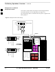
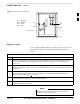
Preparing the LMF – continued LMF to BTS Connection The LMF is connected to the LAN A or B connector located on the left side of the frame’s lower air intake grill, behind the LAN Cable Access door (see Figure 3-4). Table 3-6: LMF to BTS Connection Step Action 1 To gain access to the connectors, open the LAN Cable Access door, then pull apart the Velcro tape covering the BNC “T” connector and slide out the computer service tray, if desired (see Figure 3-4).
Preparing the LMF – continued Figure 3-4: LMF Connection Detail NOTE: Open LAN CABLE ACCESS door. Pull apart Velcro tape and gain access to the LAN A or LAN B LMF BNC connector.
Preparing the LMF – continued Pinging the Processors For proper operation, the integrity of the Ethernet LAN A and B links must be be verified. Figure 3-5 represents a typical BTS Ethernet configuration. The drawing depicts one (of two identical) links, A and B. Ping is a program that sends request packets to the LAN network modules to get a response from the specified “target” module.
Preparing the LMF – continued IMPORTANT * The Ethernet LAN A and B cables must be installed on each frame/enclosure before performing this test. All other processor board LAN connections are made via the backplanes. Table 3-7: Pinging the Processors 3 Step Action 1 From the Windows desktop, click the Start button and select Run. 2 In the Open box, type ping and the GLI2 IP address (for example, ping 128.0.0.2). NOTE 128.0.0.2 is the default IP address for the GLI2 in field BTS units.
Preparing the LMF – continued Table 3-8: Logging into the BTSLMF PC Step Action 7 To use the default IP Address setting, click on Use Defaults. 8 NOTE 9 10 If this is an initial BTS optimization, the BBX Default Channels Programming Procedure must be implemented. Refer to table 2–8 for the procedure. If this is an initial BTS optimization or if a new BTS operating system release is to be loaded to the LMF, perform the steps outlined in 1 and Table 3-12.
Preparing the LMF – continued Table 3-9: Downloading Site Specific BTS Files Step Action NOTE Copy bts–#.cdf and (if they exist) bts–#.cal files to the /usr/lmf/bts–# directory. (# equates to the actual BTS site number). Unless sites use different device loads, create links to device files (as described in Table 3-10) rather than placing individual copies into each bts directory. 3 6 If files are compressed, use the uncompress *.Z command to unpack files.
Preparing the LMF – continued Table 3-10: Downloading and linking master–bts–cdma directory files for device loads Step Action NOTE File naming conventions for all processor boards and applicable files for each are listed below. Rename files using the mv UNIX command as required: Device File Name(s) 4 GLI –gliboot.hex & gli.dds BBX –bbxboot.hex & bbx.dds BDC –bdcboot.hex & bdc.dds MCC –mccboot.hex.0501 & mcc.dds.0501 CSM –csmboot.
Preparing the LMF – continued Create BTS Specific CDF File Follow the steps outlined in Table 3-11 to create a BTS specific CDF file, if one cannot be obtained from the OMCR/CBSC. (This is an interim procedure and is subject to change). Table 3-11: Create BTS Specific CDF File Step Action ! CAUTION 3 If you are not familiar with the UNIX vi editor, create a “dummy” CDF file, and practice making changes to it, prior to altering the “real” one.
Preparing the LMF – continued Update BTS Specific CDF File Device Load Version and Site Type Follow the steps outlined in Table 3-12 to update the existing BTS specific CDF file NextLoad parameter, to reflect the current device load version to be downloaded and verify the correct Site Type. (This is an interim procedure and is subject to change). CAUTION Device load version in the CDF file must match the current version loaded at the OMCR/CBSC.