Using the LMF Basic LMF Operation LMF Coverage in this Publication The LMF Application Program supports maintenance of both CDMA and SAS BTSs. All references to the LMF in this publication are to the CDMA portion of the program.. Operating Environments 3 The LMF Application Program allows the user to work in the two following Operating Environments that are accessed using the specified Desktop Icons.
Using the LMF – continued CDF/NECF Requirements For the LMF to recognize the devices installed in the BTS, a BTS CDF/NECF File that includes Equipage Information for all the devices in the BTS must be located in the applicable :\\cdma\bts–# folder. To provide the necessary Channel Assignment Data for BTS Operation, a CBSC CDF File that includes Channel Data for all BTS RF Modem Frames is also required in the folder..
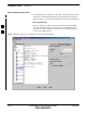
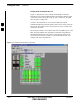
Using the LMF – continued Understanding GUI Operation The following Screen Captures are provided to help understand how the GUI operates. For detailed information on performing these and other LMF Operations, refer to the LMF Help function on–line documentation. BTS Login Screen Figure 3-5 depicts the differences between Packet and Circuit CDMA “cdf” File Identification. Note that if there is a Packet Mode Version “bts” File, the “(P)” is added as a suffix.
Using the LMF – continued Self-Managed Network Elements Screen Figure 3-6 depicts the Self-Managed Network Elements (NEs) State of a Packet Mode SC4812T. Note that an “X” is on the front of each card that is under Self–Managed Network Elements (NEs) Control by the GLI3 Card.
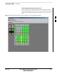
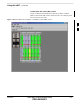
Using the LMF – continued Packet Mode Commands Screen Figure 3-7 depicts three of the available Packet Mode Commands. Normally the GLI3 has Self-Managed Network Elements (NEs) Control of all cards as shown in Figure 3-6 by an “(X)”. In that state, the LMF may only status a single card. In order to download code or test a card, the LMF must request Self-Managed Network Elements (NEs) Control of the card by using the shown Pull–down Menu.
Using the LMF – continued Packet Mode Site under LMF Control Figure 3-8 depicts a Packet Mode Site that has the MCC–1 and the BBX–1 Cards under LMF Control. Notice that the “X” is missing from the front of these two cards.
Using the LMF – continued Command Line Interface Overview The LMF also provides Command Line Interface (CLI) capability. Activate the CLI by clicking on a Shortcut Icon on the Desktop. The CLI can not be launched from the GUI, only from the Desktop Icon. Both the GUI and the CLI use a program known as the Handler. Only one Handler can be running at one time. The architectural design is such that the GUI must be started before the CLI if you want the GUI and CLI to use the same Handler.
Using the LMF – continued Prerequisites Before attempting to log into a BTS, ensure that the following tasks have been completed: S The LMF Program is correctly installed on the LMF Computer. S A bts-nnn Folder with the correct CDF/NECF and CBSC Files is present. S The LMF Computer was connected to the BTS before starting the Windows Operating System and the LMF Software. If necessary, restart the computer after connecting it to the BTS in accordance with Table 3-6 and Figure 3-3.
Using the LMF – continued Table 3-10: BTS GUI Login Procedure n Step Action * IMPORTANT The following statements are provided to assist the operator in using the LMF GUI. S If an attempt is made to log into a BTS that is already logged on, all devices will appear gray in the display. S There may be instances where the BTS initiates a log out due to a system error (i.e., a device 3 failure).
Using the LMF – continued Table 3-10: BTS GUI Login Procedure n Step 11 Action In the Equipage Information Field, select the Multi-channel Preselector Type from the Multi-channel Preselector Pull–down Menu (default is MPC) to a device corresponding to your BTS Configuration, if required. NOTE The “Use a Tower Top Amplifier” Option is not applicable to the SC4812T Lite. 12 3 In the SC4812ET Lite/T Lite Field, click in the SC4812T Lite Check Box to select it.
Using the LMF – continued BTS Login from the CLI Environment Perform the procedures in Table 3-11 to log into a BTS when using the CLI Environment. NOTE If the CLI and GUI Environments are to be used at the same time, the GUI must be started first and the BTS Login must be performed from the GUI. – Refer to Table 3-10 to start the GUI Environment and log into a BTS.
Using the LMF – continued Logging Out Logging out of a BTS is accomplished differently for the GUI and CLI Operating Environments. NOTE The GUI and CLI Environments use the same connection to a BTS. – If a GUI and the CLI Session are running for the same BTS at the same time, logging out of the BTS in either environment will log out of it for both. When either a Login or logout is performed in the CLI Window, there is no GUI indication that the Login or Logout has occurred.
Using the LMF – continued Logging Out of a BTS from the CLI Environment Perform the procedure in Table 3-13 to logout of a BTS when using the CLI Environment. Table 3-13: BTS CLI Logout Procedure n Step Action NOTE 3 If the BTS is also logged into from a GUI running at the same time and further work must be done with it in the GUI, proceed to Step 1. 1 Log out of a BTS by entering the following command: logout bts– – A system response similar to the following will be displayed: LMF> 13:24:51.
Using the LMF – continued Table 3-14: Establishing MMI Communication Procedure n Step Action 2 If the LMF Computer has only one Serial Port (COM1) and the LMF is running, disconnect the LMF from COM1 by performing the following actions. 2a Click on Tools in the LMF Window Menu Bar, and select Options from the Pull–down Menu. – An LMF Options Dialog Box will appear. 2b In the LMF Options Dialog Box, click the Disconnect Port Button on the Serial Connection Tab.
Pinging the Processors Pinging the BTS For proper operation, the integrity of the 10Base–2 Ethernet LAN A and B Links must be verified. Figure 3-10 represents a typical BTS Ethernet Configuration for an SC4812T Lite Stand–alone Frame. The drawing depicts cabling and terminators for both the A and B LANs. ”Ping” is a program that sends Request Data Packets to hosts on a network, in this case GLI Cards on the BTS LAN, to obtain a response from the “Target” Host specified by an IP Address.
Pinging the Processors – continued NOTE The Ethernet LAN A and B Cables and/or Terminators must be installed on each BTS Frame/Enclosure External LAN Connector before performing this test. All other Processor Card LAN Connections are made through the backplanes. 3 Table 3-15: Pinging the Processors Procedure n Step Action 1 If this is a first–time communication with a newly–installed frame or a GLI Card that has been replaced: – Perform the procedure in Table 6-4. – Then, return to Step 2.
Pinging the Processors – continued Table 3-15: Pinging the Processors Procedure n Step 10 Action Reset and re–Ping the target MGLI. S If the GLI does respond, proceed to Step 19. S If the GLI does not respond, typical problems to check are as follows: – – – – – 3 Failure of the LMF to Login.
Download the BTS Overview Before a BTS can operate, each equipped device must contain Device Initialization (ROM) Code. ROM Code is loaded in all devices during manufacture, factory repair, or, for software upgrades, from the CBSC using the DownLoad Manager (DLM). Device Application (RAM) Code and Data must be downloaded to each equipped device by the user before the BTS can be made fully functional for the site where it is installed.
Download the BTS – continued The RAM Code File will be selected automatically if the file is in the :\\cdma\loads\n.n.n.n\code Folder (where n.n.n.n is the download Code Version Number that matches the “NextLoad” Parameter of the CDF File). The RAM Code File in the Code Folder must have the correct Hardware BIN Number for the device to be loaded. RAM Code can be downloaded to a device that is in any state.
Download the BTS – continued Verify GLI ROM Code Loads Devices should not be loaded with a RAM Code Version that is not compatible with the ROM Code with which they are loaded. Before downloading RAM Code and Data to the Processor Cards, perform the procedure in Table 3-16 to verify that the GLI Devices are loaded with the correct ROM Code for the Software Release used by the BSS.
Download the BTS – continued Download RAM Code and Data to MGLI and GLI Perform the procedure in Table 3-17 to download the RAM Code and Data to the MGLI and other installed GLI Devices. Prerequisites S Prior to performing these procedures, ensure that a Code File exists for each of the devices to be loaded. S The LMF Computer is connected to the BTS. 3 – Refer to Table 3-6. S The LMF Computer is logged in using the GUI Environment. – Refer to Table 3-10.
Download the BTS – continued Download RAM Code and Data to Non–GLI Devices Downloads to non–GLI Devices can be performed individually for each device or all installed devices can be downloaded with one action. NOTE – CSM Cards are RAM Code–Loaded at the factory. RAM Code is downloaded to CSM Cards only if a newer software version needs to be loaded. – When downloading to multiple devices, the download may fail for some of the devices (a time–out occurs).
Download the BTS – continued Selecting CSM Clock Source and Enabling CSM Cards CSM Cards must be enabled prior to enabling the MCC Cards. Procedures in the following two sub-sections cover the actions to accomplish this. For additional information on the CSM Subsystem, see “Clock Synchronization Manager (CSM) Subsystem Description” in the CSM System Time – GPS and HSO Verification section of this chapter.
Download the BTS – continued Table 3-19: Select CSM Clock Source Procedure n Step Action 1 Select the applicable CSM(s) for which the Clock Source is to be selected. 2 Click on Device in the BTS Menu Bar, and select CSM/MAWI > Select Clock Source... in the Pull–down Menu. – A CSM Clock Reference Source Selection Window will appear. 3 Select the applicable Clock Source in the Clock Reference Source Pick List.
Download the BTS – continued Table 3-20: Enable CSM Cards Procedure n Step Action NOTE If two CSM Cards are installed and the CSM Card in the CSM 1 Slot has enabled, the LMF CSM Cage View should show Slot CSM 1 as bright green (INS–ACT) and Slot CSM 2 as dark green (INS_STANDBY). – After the CSM Cards have been successfully enabled, ensure that the PWR/ALM LEDs are steady green (alternating green/red indicates that the card is in the Alarm State).
CSM System Time – GPS and HSO Verification Clock Synchronization Manager (CSM) Subsystem Description Overview Each BTS CSM Subsystem features two CSM Cards per RF Modem Frame. The primary function of the CSM Cards is to maintain CDMA System Time. GPS is used as the Primary Timing Reference and Synchronizes the entire Cellular System. In typical operation, the Primary CSM locks its Digital Phase Locked Loop (DPLL) Circuits to GPS Signals.
CSM System Time – GPS and HSO Verification – continued Secondary Timing References The BTS may be equipped with a High Stability Oscillator (HSO), or External 10 MHz Rubidium Source that the CSM can use as a Secondary Timing Reference. Continuous GPS Synchronization is maintained for the HSO Secondary Timing References. The CSM monitors and determines what reference to use at a given time..
CSM System Time – GPS and HSO Verification – continued Table 3-22: CSM Card PWR/ALM LED States LED State Device Status Alternating Fast Flashing RED/ Slow Flashing GREEN OOS_RAM Mode and attempting to lock on to the GPS Signal. – An alarm is being reported. Solid YELLOW After a reset, the CSMs begin to boot. Color during the SRAM Test and the Flash EPROM Code Check Test. – If SRAM or Flash EPROM Tests fail, the LED changes to Steady RED and the CSM attempts to reboot. OFF FEB 2005 1.
CSM System Time – GPS and HSO Verification – continued High Stability Oscillator (HSO) The CSM and the HSO The CSM performs the overall Configuration and Status Monitoring Functions for the HSO. In the event of GPS failure, the HSO is capable of maintaining Synchronization initially established by the GPS Reference Signal.. 3 HSO The HSO is a High Stability 10 MHz oscillator with the necessary interface to the CSM Cards.
CSM System Time – GPS and HSO Verification – continued Test Equipment Set–up (GPS and HSO Verification) Perform the procedure in Table 3-23 to set–up Test Equipment. Table 3-23: Test Equipment Set–up (GPS and HSO Verification) Procedure Step Action 1 Perform one of the following as required by installed equipment: 1a For Local GPS (RF–GPS): Verify that a CSM Card with a GPS Receiver is installed in the Primary CSM Slot, CSM 1, and that the card is INS_ACTIVE (bright green).
CSM System Time – GPS and HSO Verification – continued Figure 3-11: CSM MMI Terminal Connection REFERENCE OSCILLATOR CSM Card shown removed from frame SERIAL PORT 3 EVEN SECOND TICK TEST POINT REFERENCE GPS RECEIVER ANTENNA INPUT ANTENNA COAX CABLE GPS RECEIVER 19.6 MHZ TEST POINT REFERENCE (NOTE 1) NULL MODEM BOARD (TRN9666A) 9–PIN TO 9–PIN RS–232 CABLE FW00372 LMF NOTEBOOK DB9–TO–DB25 ADAPTER COM1 NOTES: 1.
CSM System Time – GPS and HSO Verification – continued GPS Initialization/Verification Prerequisites Ensure the following prerequisites have been met before proceeding: – The Primary CSM and HSO (if equipped) has been warmed–up for at least 15 minutes. – The LMF Computer is connected to the MMI Port of the Primary CSM as shown in Figure 3-11. – An MMI Communication Session has been started (Table 3-14), and the CSM> Prompt is present in the HyperTerminal Window (Table 3-23).
CSM System Time – GPS and HSO Verification – continued Table 3-24: GPS Initialization/Verification Procedure n Step 3 Action If the HSO does not appear as one of the sources, then configure the HSO as a Back–up Source by entering the following command at the CSM> Prompt. csm>ss 1 12 – After a maximum of 15 minutes, the Rubidium Oscillator should reach operational temperature and the PWR/ALM LED on the HSO should now have changed from red to green. 3 S If the LED is green, proceed to Step 5.
CSM System Time – GPS and HSO Verification – continued Table 3-24: GPS Initialization/Verification Procedure n Step 10 Action Verify that the following GPS information (underlined text in Step 6) is true. – The GPS is usually the “0” Reference Source. – At least one Primary Reference Source must indicate “Status = good” and “Valid = yes” to bring the site up. 11 Enter the following command at the CSM> Prompt to verify that the GPS Receiver is in Tracking Mode.
CSM System Time – GPS and HSO Verification – continued Table 3-24: GPS Initialization/Verification Procedure n Step Action 13 Record the current position Base Site Latitude, Longitude, Height and Height Reference (Height Reference to Mean Sea Level (MSL) or GPS Height (GPS): GPS = 0 MSL = 1. 14 If Steps 1 through 12 pass, the GPS is good.
CSM System Time – GPS and HSO Verification – continued Table 3-24: GPS Initialization/Verification Procedure n Step 18 Action Verify the following GPS information (underlined text in Step 17, from left to right): – Lower Limit Offset from Tracked Source Variable is not less than –60 (equates to 3µs Limit). – Upper Limit Offset from Tracked Source Variable is not more than +60 (equates to 3µs Limit). – TK SRC: 0 is selected, where SRC 0 = GPS.
CSM System Time – GPS and HSO Verification – continued Connecting Test Equipment to the BTS The following types of Test Equipment are required to perform Calibration and ATP Tests: S LMF S Communications System Analyzer Model supported by the LMF S Power Meter Model supported by the LMF (required when using the 3 HP 8921A/600 and Advantest R3465 Analyzers) S Non–radiating Transmit Line Termination Load S Directional Coupler and In–line Attenuator S RF Cables and Adapters Refer to Table 3-25 for an ov
CSM System Time – GPS and HSO Verification – continued IS–95A/B Operation Optimization and ATP Testing for IS–95A/B Sites and Carriers may be performed using the following Test Equipment: S CyberTest S Advantest R3267 Spectrum Analyzer with R3562 Signal Generator S Advantest R3465 Spectrum Analyzer with R3561L Signal Generator and HP–437B or Gigatronics Power Meter S Agilent E4406A Transmitter Test Set with E4432B Signal Generator S Agilent 8935 Series E6380A Communications Test Set (formerly HP 8935)
CSM System Time – GPS and HSO Verification – continued IS–95A/B–only Test Equipment Connections Table 3-25 depicts the Interconnection Requirements for currently available Test Equipment supporting IS–95A/B only that meets Motorola Standards and is supported by the LMF. Table 3-25: IS–95A/B–only Test Equipment Interconnection COMMUNICATIONS SYSTEM ANALYZER 3 SIGNAL EVEN SECOND SYNCHRONIZATION 19.
CSM System Time – GPS and HSO Verification – continued CDMA2000 1X/IS–95A/B–capable Test Equipment Connections Table 3-26 depicts the Interconnection Requirements for currently available Test Equipment supporting both CDMA 2000 1X and IS–95A/B that meets Motorola Standards and is supported by the LMF. Table 3-26: CDMA2000 1X/IS–95A/B Test Equipment Interconnection COMMUNICATIONS SYSTEM ANALYZER ADDITIONAL TEST EQUIPMENT 3 SIGNAL EVEN SECOND SYNCHRONIZATION 19.
CSM System Time – GPS and HSO Verification – continued Equipment Warm-up NOTE To assure BTS stability and contribute to Optimization accuracy of the BTS, warm-up the BTS Test Equipment prior to performing the BTS Optimization Procedure as follows: – Agilent E7495A for a minimum of 30 minutes – All other Test Sets for a minimum of 60 minutes Time spent running initial or normal Power-up, Hardware/ Firmware Audit, and BTS Download counts as Warm-up Time.
CSM System Time – GPS and HSO Verification – continued Figure 3-12: IS–95A/B Cable Calibration Test Set–up – CyberTest, Agilent 8935, Advantest R3465, and HP 8921A SUPPORTED TEST SETS CALIBRATION SET–UP A. SHORT CABLE CAL Motorola CyberTest ÎÎÎÎ ÎÎÎÎ ÎÎÎÎÏ ANT IN SHORT CABLE TEST SET RF GEN OUT Note: The 30 dB Directional Coupler is not used with the Cybertest Test Set. The TX cable is connected directly to the Cybertest Test Set. B.
CSM System Time – GPS and HSO Verification – continued Figure 3-13: IS–95A/B and CDMA 2000 1X Cable Calibration Test Set–up – Agilent E4406A/E4432B and Advantest R3267/R3562 SUPPORTED TEST SETS CALIBRATION SET–UP A. SHORT CABLE CAL Agilent E4432B (Top) and E4406A (Bottom) SHORT CABLE TEST SET 3 RF OUTPUT 50 Ω B.
CSM System Time – GPS and HSO Verification – continued Figure 3-14: CDMA2000 1X Cable Calibration Test Set–up – Agilent 8935/E4432B SUPPORTED TEST SETS CALIBRATION SET–UP A. SHORT CABLE CAL Agilent E4432B (Top) and 8935 Series E6380A (Bottom) SHORT CABLE TEST SET 3 RF OUTPUT 50 Ω ÁÁ ÁÁ ÁÁ ÁÁ B.
CSM System Time – GPS and HSO Verification – continued Figure 3-15: CDMA2000 1X Cable Calibration Test Set–up – Agilent E7495A SUPPORTED TEST SETS Agilent E7495A CALIBRATION SET–UP A. SHORT CABLE CAL 10 DB PAD SHORT CABLE 3 TEST SET 10 DB PAD D. RX and TX TEST SET–UP 50 Ω ΤERM.
CSM System Time – GPS and HSO Verification – continued Set-up for TX Calibration Figure 3-16 and Figure 3-17 show the Test Set Connections for TX Calibration. Figure 3-16: TX Calibration Test Set–up – CyberTest (IS–95A/B) and Agilent 8935 (IS–95A/B and CDMA2000 1X) TEST SETS TRANSMIT (TX) SET–UP Motorola CyberTest ÎÎÎÎ ÎÎÎÎ ÎÎÎÎÏ FRONT PANEL POWER SENSOR NOTE: IF BTS IS EQUIPPED WITH DRFS (DUPLEXED RX/TX SIGNALS), CONNECT THE TX TEST CABLE TO THE DRF ANTENNA CONNECTOR. 100–WATT (MIN.
CSM System Time – GPS and HSO Verification – continued Figure 3-17: TX Calibration Test Set–up – Using Power Meter TEST SETS TRANSMIT (TX) SET–UP NOTE: THE HP 8921A AND ADVANTEST R3465 CANNOT BE USED FOR TX CALIBRATION. A POWER METER MUST BE USED. POWER SENSOR NOTE: IF BTS IS EQUIPPED WITH DRFS (DUPLEXED RX/TX SIGNALS), CONNECT THE TX TEST CABLE TO THE DRF ANTENNA CONNECTOR. 3 POWER METER 100–WATT (MIN.) NON–RADIATING RF LOAD TX TEST CABLE DIRECTIONAL COUPLER (30 DB) 50 Ω TERM .
CSM System Time – GPS and HSO Verification – continued Figure 3-18: TX Calibration Test Set–up – Agilent E4406A and Advantest R3567 (IS–95A/B and CDMA2000 1X) TEST SETS TRANSMIT (TX) SET–UP Agilent E4406A POWER SENSOR NOTE: IF BTS IS EQUIPPED WITH DRFS (DUPLEXED RX/TX SIGNALS), CONNECT THE TX TEST CABLE TO THE DRF ANTENNA CONNECTOR. RF INPUT 50 Ω OR INPUT 50 Ω 100–WATT (MIN.
CSM System Time – GPS and HSO Verification – continued Figure 3-19: TX Calibration Test Set–up – Agilent E7495A (IS–95A/B and CDMA2000 1X) TEST SETS TRANSMIT (TX) SET–UP Agilent E7495A POWER SENSOR NOTE: IF BTS IS EQUIPPED WITH DUPLEXED RX/TX SIGNALS, CONNECT THE TX TEST CABLE TO THE DUPLEXED ANTENNA CONNECTOR. PORT 1 RF OUT 100–WATT (MIN.) NON–RADIATING RF LOAD 3 POWER METER POWER SENSOR PORT 2 RF IN INTERNAL ETHERNET CARD TX TEST CABLE DIRECTIONAL COUPLER (30 DB) 50 Ω TERM .
CSM System Time – GPS and HSO Verification – continued Set–up for ATP Figure 3-20 and Figure 3-21 show the Test Set Connections for ATP Tests. Figure 3-20: IS–95A/B ATP Test Set–up, TRF Shown – CyberTest, Advantest R3465, and Agilent 8935 TEST SETS Optimization/ATP SET–UP Motorola CyberTest SYNC MONITOR EVEN SEC TICK PULSE REFERENCE FROM CSM BOARD FREQ MONITOR 19.
CSM System Time – GPS and HSO Verification – continued Figure 3-21: IS–95A/B ATP Test Set–up – HP 8921A TEST SETS Optimization/ATP SET–UP Hewlett Packard Model HP 8921A W/PCS Interface (for 1900 MHz) SYNC MONITOR EVEN SEC TICK PULSE REFERENCE FROM CSM BOARD IMPORTANT: WHEN PERFORMING FER TEST ON COMPANION FRAME DIVERSITY RX, CONNECT RX TEST CABLE TO RX ANTENNA PORT ON COLLOCATED COMPANION FRAME. FREQ MONITOR 19.
CSM System Time – GPS and HSO Verification – continued Figure 3-22: IS–95A/B and CDMA2000 1X ATP Test Set–up With DRFs – Agilent Test Equipment TEST SETS Optimization/ATP SET–UP Agilent E4432B (Top) and 8935 Series E6380A (Bottom) RF OUTPUT 50 Ω Á Á ÁÁ RF OUTPUT 50 Ω IMPORTANT: WHEN PERFORMING FER TEST ON COMPANION FRAME DIVERSITY RX, CONNECT RX TEST CABLE TO ANTENNA PORT ON COLLOCATED COMPANION FRAME.
CSM System Time – GPS and HSO Verification – continued Figure 3-23: IS–95A/B and CDMA2000 1X ATP Test Set–up With DRFs – Advantest R3267/3562 Test Equipment TEST SETS Optimization/ATP SET–UP IMPORTANT: WHEN PERFORMING FER TEST ON COMPANION FRAME DIVERSITY RX, CONNECT RX TEST CABLE TO ANTENNA PORT ON COLLOCATED COMPANION FRAME.
CSM System Time – GPS and HSO Verification – continued Figure 3-24: IS–95A/B and CDMA2000 1X ATP Test Set–up With TRFs – Agilent Test Equipment TEST SETS Optimization/ATP SET–UP IMPORTANT: WHEN PERFORMING FER TEST ON COMPANION FRAME DIVERSITY RX, CONNECT RX TEST CABLE TO RX ANTENNA PORT ON COLLOCATED COMPANION FRAME.
CSM System Time – GPS and HSO Verification – continued Figure 3-25: IS–95A/B and CDMA2000 1X ATP Test Set–up With TRFs – Advantest R3267/3562 Test Equipment TEST SETS Optimization/ATP SET–UP IMPORTANT: WHEN PERFORMING FER TEST ON COMPANION FRAME DIVERSITY RX, CONNECT RX TEST CABLE TO RX ANTENNA PORT ON COLLOCATED COMPANION FRAME.
CSM System Time – GPS and HSO Verification – continued Figure 3-26: IS–95A/B and CDMA2000 1X Optimization/ATP Test Set–up – Agilent E7495A ATP TEST SET–UP TEST SET Power Meter Agilent E7495A NOTE: IF BTS IS EQUIPPED WITH DUPLEXED RX/TX SIGNALS, CONNECT THE TX TEST CABLE TO THE DUPLEXED ANTENNA CONNECTOR. RX TEST RF INPUT 50 Ω OR INPUT 50 Ω 100–WATT (MIN.
Test Equipment Set-up Connecting Test Equipment to the BTS The following types of Test Equipment are required to perform Calibration and ATP Tests: S LMF S Communications System Analyzer Model supported by the LMF S Power Meter Model supported by the LMF (required when using the 3 HP 8921A/600 and Advantest R3465 Analyzers) S Non–radiating Transmit Line Termination Load S Directional Coupler and In–line Attenuator S RF Cables and Adapters Refer to Table 3-27 for an overview of Test Equipment Connectio
Test Equipment Set-up – continued IS–95A/B Operation Optimization and ATP Testing for IS–95A/B Sites and Carriers may be performed using the following Test Equipment: S CyberTest S Advantest R3267 Spectrum Analyzer with R3562 Signal Generator S Advantest R3465 Spectrum Analyzer with R3561L Signal Generator and HP–437B or Gigatronics Power Meter S Agilent E4406A Transmitter Test Set with E4432B Signal Generator S Agilent 8935 Series E6380A Communications Test Set (formerly HP 8935) S Hewlett–Packard HP
Test Equipment Set-up – continued IS–95A/B–only Test Equipment Connections Table 3-27 depicts the Interconnection Requirements for currently available Test Equipment supporting IS–95A/B only that meets Motorola Standards and is supported by the LMF. Table 3-27: IS–95A/B–only Test Equipment Interconnection COMMUNICATIONS SYSTEM ANALYZER 3 SIGNAL EVEN SECOND SYNCHRONIZATION 19.
Test Equipment Set-up – continued CDMA2000 1X/IS–95A/B–capable Test Equipment Connections Table 3-28 depicts the Interconnection Requirements for currently available Test Equipment supporting both CDMA 2000 1X and IS–95A/B that meets Motorola Standards and is supported by the LMF. Table 3-28: CDMA2000 1X/IS–95A/B Test Equipment Interconnection COMMUNICATIONS SYSTEM ANALYZER ADDITIONAL TEST EQUIPMENT 3 SIGNAL EVEN SECOND SYNCHRONIZATION 19.
Test Equipment Set-up – continued Equipment Warm-up NOTE To assure BTS stability and contribute to Optimization accuracy of the BTS, warm-up the BTS Test Equipment prior to performing the BTS Optimization Procedure as follows: – Agilent E7495A for a minimum of 30 minutes – All other Test Sets for a minimum of 60 minutes Time spent running initial or normal Power-up, Hardware/ Firmware Audit, and BTS Download counts as Warm-up Time.
Test Equipment Set-up – continued Figure 3-27: IS–95A/B Cable Calibration Test Set–up – CyberTest, Agilent 8935, Advantest R3465, and HP 8921A SUPPORTED TEST SETS CALIBRATION SET–UP A. SHORT CABLE CAL Motorola CyberTest ÎÎÎÎ ÎÎÎÎ ÎÎÎÎÏ ANT IN SHORT CABLE TEST SET RF GEN OUT Note: The 30 dB Directional Coupler is not used with the Cybertest Test Set. The TX cable is connected directly to the Cybertest Test Set. B.
Test Equipment Set-up – continued Figure 3-28: IS–95A/B and CDMA 2000 1X Cable Calibration Test Set–up – Agilent E4406A/E4432B and Advantest R3267/R3562 SUPPORTED TEST SETS CALIBRATION SET–UP A. SHORT CABLE CAL Agilent E4432B (Top) and E4406A (Bottom) SHORT CABLE TEST SET 3 RF OUTPUT 50 Ω B.
Test Equipment Set-up – continued Figure 3-29: CDMA2000 1X Cable Calibration Test Set–up – Agilent 8935/E4432B SUPPORTED TEST SETS CALIBRATION SET–UP A. SHORT CABLE CAL Agilent E4432B (Top) and 8935 Series E6380A (Bottom) SHORT CABLE TEST SET 3 RF OUTPUT 50 Ω ÁÁ ÁÁ ÁÁ ÁÁ B. RX TEST SET–UP FOR TRF N–N FEMALE ADAPTER RX CABLE ANT IN SHORT CABLE NOTE: TEST SET 10 MHZ IN ON REAR OF SIGNAL GENERATOR IS CONNECTED TO 10 MHZ REF OUT ON SIDE OF CDMA BASE STATION TEST SET (FIGURE F-17). D.
Test Equipment Set-up – continued Figure 3-30: CDMA2000 1X Cable Calibration Test Set–up – Agilent E7495A SUPPORTED TEST SETS Agilent E7495A CALIBRATION SET–UP A. SHORT CABLE CAL 10 DB PAD SHORT CABLE 3 TEST SET 10 DB PAD D. RX and TX TEST SET–UP 50 Ω ΤERM.
Test Equipment Set-up – continued Set-up for TX Calibration Figure 3-31 and Figure 3-32 show the Test Set Connections for TX Calibration. Figure 3-31: TX Calibration Test Set–up – CyberTest (IS–95A/B) and Agilent 8935 (IS–95A/B and CDMA2000 1X) TEST SETS TRANSMIT (TX) SET–UP Motorola CyberTest ÎÎÎÎ ÎÎÎÎ ÎÎÎÎÏ FRONT PANEL POWER SENSOR NOTE: IF BTS IS EQUIPPED WITH DRFS (DUPLEXED RX/TX SIGNALS), CONNECT THE TX TEST CABLE TO THE DRF ANTENNA CONNECTOR. 100–WATT (MIN.
Test Equipment Set-up – continued Figure 3-32: TX Calibration Test Set–up – Using Power Meter TEST SETS TRANSMIT (TX) SET–UP NOTE: THE HP 8921A AND ADVANTEST R3465 CANNOT BE USED FOR TX CALIBRATION. A POWER METER MUST BE USED. POWER SENSOR NOTE: IF BTS IS EQUIPPED WITH DRFS (DUPLEXED RX/TX SIGNALS), CONNECT THE TX TEST CABLE TO THE DRF ANTENNA CONNECTOR. 3 POWER METER 100–WATT (MIN.) NON–RADIATING RF LOAD TX TEST CABLE DIRECTIONAL COUPLER (30 DB) 50 Ω TERM .
Test Equipment Set-up – continued Figure 3-33: TX Calibration Test Set–up – Agilent E4406A and Advantest R3567 (IS–95A/B and CDMA2000 1X) TEST SETS TRANSMIT (TX) SET–UP Agilent E4406A POWER SENSOR NOTE: IF BTS IS EQUIPPED WITH DRFS (DUPLEXED RX/TX SIGNALS), CONNECT THE TX TEST CABLE TO THE DRF ANTENNA CONNECTOR. RF INPUT 50 Ω OR INPUT 50 Ω 100–WATT (MIN.
Test Equipment Set-up – continued Figure 3-34: TX Calibration Test Set–up – Agilent E7495A (IS–95A/B and CDMA2000 1X) TEST SETS TRANSMIT (TX) SET–UP Agilent E7495A POWER SENSOR NOTE: IF BTS IS EQUIPPED WITH DUPLEXED RX/TX SIGNALS, CONNECT THE TX TEST CABLE TO THE DUPLEXED ANTENNA CONNECTOR. PORT 1 RF OUT 100–WATT (MIN.) NON–RADIATING RF LOAD 3 POWER METER POWER SENSOR PORT 2 RF IN INTERNAL ETHERNET CARD TX TEST CABLE DIRECTIONAL COUPLER (30 DB) 50 Ω TERM .
Test Equipment Set-up – continued Set–up for ATP Figure 3-35 and Figure 3-36 show the Test Set Connections for ATP Tests. Figure 3-35: IS–95A/B ATP Test Set–up, TRF Shown – CyberTest, Advantest R3465, and Agilent 8935 TEST SETS Optimization/ATP SET–UP Motorola CyberTest SYNC MONITOR EVEN SEC TICK PULSE REFERENCE FROM CSM BOARD FREQ MONITOR 19.
Test Equipment Set-up – continued Figure 3-36: IS–95A/B ATP Test Set–up – HP 8921A TEST SETS Optimization/ATP SET–UP Hewlett Packard Model HP 8921A W/PCS Interface (for 1900 MHz) SYNC MONITOR EVEN SEC TICK PULSE REFERENCE FROM CSM BOARD IMPORTANT: WHEN PERFORMING FER TEST ON COMPANION FRAME DIVERSITY RX, CONNECT RX TEST CABLE TO RX ANTENNA PORT ON COLLOCATED COMPANION FRAME. FREQ MONITOR 19.
Test Equipment Set-up – continued Figure 3-37: IS–95A/B and CDMA2000 1X ATP Test Set–up With DRFs – Agilent Test Equipment TEST SETS Optimization/ATP SET–UP Agilent E4432B (Top) and 8935 Series E6380A (Bottom) RF OUTPUT 50 Ω Á Á ÁÁ RF OUTPUT 50 Ω IMPORTANT: WHEN PERFORMING FER TEST ON COMPANION FRAME DIVERSITY RX, CONNECT RX TEST CABLE TO ANTENNA PORT ON COLLOCATED COMPANION FRAME. Signal Generator 10 MHZ IN PATTERN TRIG IN RX TEST CABLE Communications System Analyzer 100–WATT (MIN.
Test Equipment Set-up – continued Figure 3-38: IS–95A/B and CDMA2000 1X ATP Test Set–up With DRFs – Advantest R3267/3562 Test Equipment TEST SETS Optimization/ATP SET–UP IMPORTANT: WHEN PERFORMING FER TEST ON COMPANION FRAME DIVERSITY RX, CONNECT RX TEST CABLE TO ANTENNA PORT ON COLLOCATED COMPANION FRAME. Advantest R3267 (Top) and R3562 (Bottom) TO EXT TRIG ON REAR OF SPECTRUM ANALYZER 3 RF OUT 50 Ω Signal Generator MOD TIME BASE IN SYNTHE REF IN EXT TRIG IN GPIB RX TEST CABLE 100–WATT (MIN.
Test Equipment Set-up – continued Figure 3-39: IS–95A/B and CDMA2000 1X ATP Test Set–up With TRFs – Agilent Test Equipment TEST SETS Optimization/ATP SET–UP IMPORTANT: WHEN PERFORMING FER TEST ON COMPANION FRAME DIVERSITY RX, CONNECT RX TEST CABLE TO RX ANTENNA PORT ON COLLOCATED COMPANION FRAME.
Test Equipment Set-up – continued Figure 3-40: IS–95A/B and CDMA2000 1X ATP Test Set–up With TRFs – Advantest R3267/3562 Test Equipment TEST SETS Optimization/ATP SET–UP IMPORTANT: WHEN PERFORMING FER TEST ON COMPANION FRAME DIVERSITY RX, CONNECT RX TEST CABLE TO RX ANTENNA PORT ON COLLOCATED COMPANION FRAME.
Test Equipment Set-up – continued Figure 3-41: IS–95A/B and CDMA2000 1X Optimization/ATP Test Set–up – Agilent E7495A ATP TEST SET–UP TEST SET Power Meter Agilent E7495A NOTE: IF BTS IS EQUIPPED WITH DUPLEXED RX/TX SIGNALS, CONNECT THE TX TEST CABLE TO THE DUPLEXED ANTENNA CONNECTOR. RX TEST RF INPUT 50 Ω OR INPUT 50 Ω 100–WATT (MIN.
Test Set Calibration Test Equipment Calibration Background Proper Test Equipment Calibration helps to ensure accurate BTS Optimization and Acceptance Testing by assuring that the Test Equipment and associated cables do not introduce Measurement Errors. NOTE 3 If the Test Equipment Set being used to optimize or test the BTS has been calibrated and maintained as a set, this procedure does not need to be performed. This procedure must be performed prior to beginning the Optimization.
Test Set Calibration – continued Manual Calibration Procedures Agilent E4406A Transmitter Tester The E4406A does not support the Power Level Zeroing Calibration performed by the LMF. If this instrument is to be used for Bay Level Offset Calibration and Calibration is attempted with the LMF Calibrate Test Equipment Function, the LMF will return a Failure Message Status Window stating that Zeroing Power is not supported by the E4406A.
Test Set Calibration – continued Prerequisites Ensure that the following have been completed before selecting Test Equipment: S Test Equipment is turned on. S GPIB Addresses set in the Test Equipment have been verified as correct using the applicable procedures in Appendix F. (Not required with Agilent E7495A.) 3 S LMF Computer Serial Port and Test Equipment are connected to the GPIB Box.
Test Set Calibration – continued Table 3-29: Selecting Test Equipment Manually in the Serial Connection Tab Procedure n Step 4 Action Type the GPIB Address in the corresponding GPIB Address Box. – Refer to the Setting GPIB Addresses section of Appendix F for directions on verifying and/or changing Test Equipment GPIB Addresses.
Test Set Calibration – continued Automatically Selecting Test Equipment in the Serial Connection Tab When using the Auto–detection Feature to select Test Equipment, the LMF determines which Test Equipment Items are actually communicating with LMF. Perform the procedure in Table 3-30 to use the Auto–detection Feature. Table 3-30: Selecting Test Equipment Using Auto-Detect Procedure 3 n Step Action NOTE An alternate procedure is required if using the Agilent E7495A Test Set.
Test Set Calibration – continued Detecting Test Equipment when using Agilent E7495A IMPORTANT * Verify that no other equipment is connected to the LMF. Agilent E7495A equipment must be connected to the LAN to detect it. Then perform the procedures described in Appendix F. Specifically, refer to Table F-1 on Page F-1, Table F-2, and Table F-3 on Page F-3.
Test Set Calibration – continued LMF Cables Calibration Overview The LMF Cable Calibration Function is used to measure the Path Loss (in dB) for the TX and RX Cables, Adapters, Directional Couplers, and Attenuators that make up the Cable Configurations used for testing. A Communications System Analyzer is used to measure the Signal Loss of both the TX Test Cable and the RX Test Cable Configurations.
Test Set Calibration – continued Calibrating Test Cabling using a Communications System Analyzer Prerequisites S Test Equipment is turned on and has warmed–up for at least 60 minutes. S Test Equipment has been selected in the LMF (Table 3-29 or 3 Table 3-30). S Test Equipment has been calibrated and correctly connected for the type of Test Cable Configuration to be calibrated. NOTE LMF Cable Calibration cannot be accomplished with an HP 8921A Analyzer for 1.9 GHz.
Test Set Calibration – continued Table 3-32: Test Cabling Calibration using Communications System Analyzer Procedure n Step 3 Action Select: – TX and RX CABLE CAL, TX CABLE CAL or – RX CABLE CAL in the Cable Calibration Pick List. 3 4 Click OK, and follow the directions displayed for each step. – A Status Report Window will be displayed with the results of the Cable Calibration.
Test Set Calibration – continued Calibrate Test Cabling using a Signal Generator and Spectrum Analyzer Refer to Figure 3-42 and perform the procedure in Table 3-33 to calibrate the TX Test Cable Configuration for all BTSs or the RX ATP Test Cable Configuration for BTSs with Duplexed TX/RX using the Signal Generator and Spectrum Analyzer.
Test Set Calibration – continued Figure 3-42: Calibration Set–up for TX/Duplexed RX Test Cabling using a Signal Generator and a Spectrum Analyzer THIS WILL CONNECT TO THE BTS TX ANTENNA CONNECTOR DURING TX CALIBRATION AND TO THE TX/RX ANTENNA CONNECTORS DURING ATP TESTS. Signal Generator Spectrum Analyzer 40W NON–RADIATING RF LOAD 3 Signal Generator A SHORT TEST CABLE 50 OHM TERMINATOR 20DB 20 W IN–LINE ATTENUATOR FOR 1.
Test Set Calibration – continued Table 3-34: Non–Duplexed RX Test Cabling Using Signal Generator and Spectrum Analyzer Calibration Procedure n Step 4 Action Change the Test Set–up to the one shown in Detail “B” (lower portion of Figure 3-43) to measure the output at the Customer’s RX Frequency. – 824.7–848.31 MHz for North American Cellular or – 1850–1910 MHz for North American PCS 5 Record the value measured with the Detail “B” Test Set–up.
Test Set Calibration – continued Setting Cable Loss Values Cable Loss Values for TX and RX Test Cable Configurations are normally set by accomplishing Automatic Cable Calibration using the LMF and the applicable Test Equipment. The LMF stores the measured Signal Loss Values in the Test Cable Insertion Loss Files. The Test Cable Insertion Loss Values can also be set or changed manually.
Test Set Calibration – continued Setting TX Coupler Loss Value If an in–service TX Coupler is installed, the Coupler Loss must be manually entered so it will be included in the LMF TX Calibration and Audit Calculations. Prerequisites S LMF is logged into the BTS. S Path Loss, in dB, of the TX Coupler must be known. 3 Table 3-36: Setting TX Coupler Loss Values Procedure n Step 1 Action Click Util in the BTS Menu Bar, and select Edit > Coupler Loss... in the Pull–down Menus.
Bay Level Offset Calibration Introduction Bay Level Offset (BLO) Calibration is the central activity of the Optimization Process. BLO Calibration compensates for normal equipment variations within the BTS RF Paths and assures that the correct Transmit Power is available at the BTS Antenna Connectors to meet site performance requirements. 3 What is BLO Calibration? Description BLO Calibration is the complete title of what is normally referred to as “Calibration.
Bay Level Offset Calibration – continued S Expansion Frame Diversity RX Path – The Starter Frame Main RX Signal is used for the Expansion Frame Diversity RX Signal. An Expansion Frame’s Diversity RX Path starts at ANTENNAS Connectors 1A, 2A, or 3A in the Starter Frame. It travels through the associated TRF or DRF, the MPC in SCCP Cage MPC–1 Slot, and the CIO Card where it is then routed out of the frame through the RX Expansion Out Connectors (RX EXPANSION 1A, 2A, or 3A).
Bay Level Offset Calibration – continued – TX Filter or TX Filter Combiner – TX Filter/Filter Combiner–to–DRF/TRF Cable – DRF or TRF BLO Calibration Data File During the Calibration Process, the LMF creates a Calibration (CAL) Data File where BLO Values are stored. After Calibration has been completed, these Offset Values must be downloaded to the BBX Cards using the LMF BLO Download Function. A detailed description of the file organization and content is provided in the following paragraphs.
Bay Level Offset Calibration – continued S The first view of the array is shown in Table 3-37. This view shows the three branches of the array (Transmit, Main Receive, and Diversity Receive Offsets, and the Calibration Entry ranges that apply to each. Table 3-37: BLO bts–#.
Bay Level Offset Calibration – continued Table 3-38: SC4812T Lite bts–#.
Bay Level Offset Calibration – continued Example: C[1]=384 C[2]=19102 (Even Cal Entry) C[3]=777 (Odd Cal Entry) C[4]=19086 (Even Cal Entry) (Odd Cal Entry) = 1 “Calibration Point” = 1 “Calibration Point” . . . C[19]=777 3 (Odd Cal Entry) C[20]=19086 (Even Cal Entry) = 1 “Calibration Point” In the example above, BLO was measured at only two frequencies (Channels 384 and 777) for SCCP BBX–1 Slot Transmit (Table 3-38).
Bay Level Offset Calibration – continued Table 3-39: Set–up Test Equipment for RF Path Calibration Procedure n Step Action ! CAUTION To prevent damage to the Test Equipment, all Transmit (TX) Test Connections must be via the 30 dB Directional Coupler for 800 MHz or via a 30 dB Coupler with a 20 dB In–line Attenuator for 1900 MHz. 4 3 For TX Path Calibration, connect the Test Equipment as shown in Figure 3-16, Figure 3-17, or Figure 3-18, depending on the Communications Analyzer being used.
Bay Level Offset Calibration – continued Example: Measured Power Input (at TX Port) = 39.0 dBm Known BBX TX Power Output = –6.0 dBm BLO = (39.0) – (–6.0) = 45.0 dB Gain TX Calibration and the LMF The LMF Tests > TX > TX Calibration... and Tests > All Cal/Audit... Selections perform TX BLO Calibration Testing for installed BBX(s). – The All Cal/Audit... Selection initiates a series of actions to perform TX Calibration, and if Calibration is successful, download BLO and perform TX Audit.
Bay Level Offset Calibration – continued Primary BBX Cards normally will have BLOs in the lower half of the range. Using the example range, this would be from 40 to 45 dB. Checking the Single–Sided BLO Check Box should only be done when calibrating Primary BBX Cards because it will reduce the acceptable BLO Value variations to the lower half of the range.
Bay Level Offset Calibration – continued Test Pattern Channels and Gain Settings – The CDMA Channels and their respective Digital Gain Settings used for each Test Pattern are listed in Table 3-40.
Bay Level Offset Calibration – continued NOTE At new site installations, to facilitate the complete test of each SCCP Cage (if the cage is not already fully populated with BBX Cards), move BBX Cards from shelves currently not under test and install them into the empty BBX Slots of the shelf currently being tested to insure that all BBX TX Paths are tested. – This procedure can be bypassed on operational sites that are due for periodic Optimization.
Bay Level Offset Calibration – continued Table 3-41: All Cal/Audit and TX Calibration Procedure n Step Action 1 If it has not already been done, configure the Test Equipment for TX Calibration by performing the procedure in Table 3-39. 2 Click on the BBX(s) to be calibrated. 3 If the Test Pattern to be used is Standard, CDFPilot, or CDF, select at least one MCC. – Refer to “Test Pattern Drop–down Pick List” under “TX Calibration and the LMF” in this section. 4 For All Cal Audit...
Bay Level Offset Calibration – continued Table 3-41: All Cal/Audit and TX Calibration Procedure n 3 Step Action 10 In the Test Pattern Box, select the Test Pattern to use for the Calibration from the Pull–down Menu. – Refer to “Test Pattern Drop–down Pick List” under “TX Calibration and the LMF” in this section. 11 Click OK to display the Status Report Window. – A Directions Pop-up Window will then appear. 12 Follow the Cable Connection Directions as they are displayed.
Bay Level Offset Calibration – continued Table 3-42: Download BLO Data Procedure n Step Action 1 Select the BBX(s) to be downloaded. 2 Click Device in the BTS Menu Bar, and select Download > BLO from the Pull–down Menus. – A Status Report Window displays the result of the download. NOTE 3 Selected device(s) do not change color when BLO is downloaded. 3 Click OK to close the Status Report Window.
Bay Level Offset Calibration – continued TX Audit Test The Tests Menu Item, TX Audit, performs the TX BLO Audit Test for BBX Cards. All measurements are made through the appropriate TX Output Connector using the TX Calibration Set–up. Prerequisites Before running this test, the following should be done: 3 S The CSM 1 Card, GLI Cards, and BBX Cards all have the correct Code Load. S The Primary CSM and MGLI Cards are INS_ACTIVE (bright green). S All BBX Cards are OOS_RAM (yellow).
Bay Level Offset Calibration – continued Table 3-43: BTS TX Path Audit Procedure n Step 6 Action Verify that the correct Channel Number for the selected carrier is shown in the Carrier # Channels Box. S If it is not, obtain the latest bts–#.cdf (or bts–#.necf) and cbsc–#.CDF Files from the CBSC. NOTE If necessary, the correct Channel Number may be manually entered into the Carrier # Channels Box.
Bay Level Offset Calibration – continued After a BTS has been fully optimized a copy of the CAL File must be present so it can be transferred to the CBSC. S If TX Calibration has been successfully performed for all BBX Cards and BLO Data has been downloaded, a CAL File will exist. NOTE The Create Cal File Function only applies to selected (highlighted) BBX Cards. 3 CAUTION Editing the CAL File is not encouraged because this action can cause interface problems between the BTS and the LMF.
RFDS Set–up and Calibration RFDS Description The optional RFDS is used to perform RF Tests of the site from the CBSC or from the LMF. The RFDS contains the following FRUs: S Antenna Select Unit (ASU) S Fixed Wireless Terminal Interface Card (FWTIC) S Subscriber Unit Assembly (SUA) For complete information regarding the RFDS, refer to the CDMA CDMA RFDS Hardware Installation; 68P64113A93, CDMA RFDS User’s Guide; 68P64114A51, and the LMF Help function on–line documentation. RFDS Parameters The bts–#.
RFDS Set–up and Calibration – continued Checking and Setting RFDS Parameters Perform the procedure in Table 3-45 to review and/or edit RFDS Parameters. Table 3-45: RFDS Parameter Settings Procedure n Step 3 Action NOTE Log out of the BTS prior to perform this procedure. 1 Using a Text Editor, verify that the following fields are set correctly in the bts–#.cdf File.
RFDS Set–up and Calibration – continued Table 3-45: RFDS Parameter Settings Procedure n Step 5c Action Click on Device in the BTS Menu Bar, and select Disable from the Pull–down Menu. – A Status Report Window shows the status of the operation. 5d When the operation is complete, click OK to close the Status Report Window. 5e Click on the MGLI [now OOS_RAM (yellow)]. 5f Click on Device in the BTS Menu Bar, and select Download > Data from the Pull–down Menus.
RFDS Set–up and Calibration – continued Table 3-45: RFDS Parameter Settings Procedure n Step Action 6c Click OK to close the Status Report Window. 6d Repeat Step 6a to select the MCC Cards. 6e Click on Device in the BTS Menu Bar and select Download > Data from the Pull–down Menu. – A Status Report Window shows the status of the download. 3 NOTE Selected devices do not change color when data is downloaded. 6f Click on OK to close the Status Report Window.
RFDS Set–up and Calibration – continued RFDS TSU NAM Programming The Number Assignment Module (NAM) information needs to be programmed into the TSU before it can receive and process Test Calls, or be used for any type of RFDS Test. The RFDS TSU NAM must be programmed with the appropriate system parameters and a phone number during hardware installation. The TSU Phone Number and TSU MSI must be recorded for each BTS used for OMC–R RFDS Software Configuration.
RFDS Set–up and Calibration – continued Valid NAM Ranges Table 3-47 provides the valid NAM Field Ranges. If any of the fields are missing or out-of–range, the RFDS will error out.
RFDS Set–up and Calibration – continued Set Antenna Map Data The Antenna Map Data must be entered manually if an RFDS is installed. Antenna Map Data does not need to be entered if an RFDS is not installed. The Antenna Map Data is only used for RFDS Tests and is required if an RFDS is installed. Prerequisite S The LMF is logged into the BTS. 3 Perform the procedure in Table 3-48 to set Antenna Map Data for the RFDS.
RFDS Set–up and Calibration – continued Set RFDS Configuration Data If an RFDS is installed, the RFDS Configuration Data must be manually entered. Prerequisite S LMF is logged into the BTS 3 NOTE The entered antenna# index numbers must correspond to the antenna# index numbers used in the Antenna Maps. Perform the procedure in Table 3-49 to set RFDS Configuration Data.
RFDS Set–up and Calibration – continued RFDS Calibration The RFDS Calibration option is used to calibrate the RFDS TX and RX Paths. TX Path Calibration For a TX Antenna Path Calibration, the BTS XCVR is keyed at a pre–determined Power Level and the BTS Power Output Level is measured by the RFDS. The Power Level is then measured at the TX Antenna Directional Coupler by the power measuring Test Equipment Item being used (Power Meter or Analyzer).
RFDS Set–up and Calibration – continued Prerequisites S Test Equipment has been selected. S Test Equipment and Test Cables have been calibrated. S TX Calibration has been performed and BLO Data has been downloaded to the BBX Cards. S Test Equipment and Test Cables are connected for TX Calibration. S Antenna Map Data has been entered for the site. S BBX Cards are OOS–RAM. 3 RFDS Calibration Procedure Perform the procedure in Table 3-51 to perform RFDS Calibration.
RFDS Set–up and Calibration – continued Table 3-51: RFDS Calibration Procedure n Step 10 Action Click on the OK Button. – A Status Report Window is displayed, followed by a Directions Pop–up Window. 11 Follow the Cable Connection Directions as they are displayed. 12 When the test is completed, the test results are displayed in the Status Report Window. 13 Click on the OK Button to close the Status Report Window. 14 Click on the BTS Frame Tab. 15 Select the MGLI by clicking on it.
Alarms Testing Alarm Verification ALARM Connectors provide Customer Defined Alarm Inputs and Outputs. The customer can connect BTS Site Alarm Input Sensors and Output Devices to the BTS, thus providing Alarm Reporting from active sensors as well as controlling Output Devices. The SC 4812T Lite is capable of concurrently monitoring 35 Iinput Signals. These Input Signals are divided between two Alarm Connectors marked ‘ALARM A’ and ‘ALARM B’ located at the top of the frame. Refer to Figure 3-44.
Alarms Testing – continued Alarm A and Alarm B Connector Comparison The ALARM A Connector is always functional; the ALARM B Connector is functional when an AMR Card is equipped in the AMR 2 Slot in the SCCP Cage. Refer to Figure 3-45. The ALARM A Port monitors Input Numbers 1 through 9 and 11 through 18, while ALARM B Port monitors Input Numbers 19 through 36. Refer to Figure 3-46. – Alarm 10 is reserved for system use.
Alarms Testing – continued Figure 3-46: AMR Connector Pin Numbering A CDI 18 ... A CDI 1 Returns 60 26 2 60 26 2 59 25 1 59 25 1 Returns 3 ALARM A (AMR 1) B CDI 36 ... ALARM B (AMR 2) B CDI 19 FW00302 Alarm Reporting Display The Alarm Monitor Window can be displayed to list alarms that occur after the window is displayed. To access the Alarm Monitor Window, select Util>Alarm Monitor.
Alarms Testing – continued Study the Site Engineering Documents and perform the following tests only after first verifying that the AMR Cabling Configuration required to interconnect the BTS Frame with External Alarm Sensors and/or Relays meet requirements stated in the 1X SC4812T Lite Hardware Installation manual (68P09262A57) Manual. NOTE Motorola highly recommends that before you start this procedure, you read and understand it in its entirety.
Alarms Testing – continued Table 3-53: CDI Alarm Input Verification Procedure (using the Alarms Test Box) n Step 3 Action 1 Connect the LMF to the BTS. 2 Log into the BTS. 3 Select the MGLI. 4 Click on the Device Menu. 5 Click on the Set Alarm Relays Menu Item. 6 Click on Normally Open. – A Status Report Window displays the results of the action. 7 Click on the OK Button to close the Status Report Window. 8 Set all switches on the Alarms Test Box to the Open position.
Alarms Testing – continued Table 3-53: CDI Alarm Input Verification Procedure (using the Alarms Test Box) n Step 21 Action Click OK to close the Status Report Window. – Alarms should be reported for Alarm Inputs 1 through 36. 22 Set all switches on the Alarms Test Box to the Closed position. 23 Connect the Alarms Test Box to the ALARM A Connector. 3 – Alarms should be reported for Alarm Inputs 1 through 18. 24 Set all switches on the Alarms Test Box to the Open position.
Alarms Testing – continued Table 3-53: CDI Alarm Input Verification Procedure (using the Alarms Test Box) n Step Action 41 Disconnect the Alarms Test Box from the ALARM B Connector. 42 Load data to the MGLI to reset the Alarm Relay Conditions according to the CDF File. 3 CDI Alarm Input Verification without Alarms Test Box Table 3-54 describes how to test the CDI Alarm Input verification without the use of the Alarms Test Box. Follow the steps as instructed and compare results with the LMF Display.
Alarms Testing – continued Table 3-54: CDI Alarm Input Verification Procedure (without the Alarms Test Box) n Step Action 9 Refer to Figure 3-46 and sequentially short the ALARM B Connector CDI 19 through CDI 36 pins (25–26 through 59–60) together. – An alarm should be reported for each pair of pins that are shorted. – An Alarm Clear Message should be reported for each pair of pins when the short is removed. 10 Select the MGLI. 11 Click on the Device Menu.
Alarms Testing – continued Table 3-54: CDI Alarm Input Verification Procedure (without the Alarms Test Box) n Step Action 23 Refer to Figure 3-46 and sequentially short the ALARM B Connector CDI 19 through CDI 36 pins (25–26 through 59–60) together. – No alarms should be displayed. 24 Load data to the MGLI to reset the Alarm Relay Conditions according to the CDF File. 3 Pin and Signal Information for Alarm Connectors Table 3-55 lists the Pins and Signal Names for Alarms A and B.
Alarms Testing – continued Table 3-55: Pin and Signal Information for Alarm Connectors ALARM A Pin Signal Name Pin ALARM B Signal Name Pin Signal Name Pin Signal Name 19 A CDO7 NC 49 Cust Retn 13 19 B CDO15 NC 49 B CDI 31 20 A CDO7 Com 50 A CDI 13 20 B CDO15 Com 50 Cust Retn 31 21 A CDO7 NO 51 Cust Retn 14 21 B CDO15 NO 51 B CDI 32 22 A CDO8 NC 52 A CDI 14 22 B CDO16 NC 52 Cust Retn 32 23 A CDO8 Com 53 Cust Retn 15 23 B CDO16 Com 53 B CDI 33 24 A CDO8 NO 5
Alarms Testing – continued Notes 3 3-150 1X SC 4812T Lite BTS Optimization/ATP PRELIMINARY FEB 2005