After Sales Technical Documentation BOOSTER KIT BSH–1 Original, 09/94 NMP Part No.
Booster Kit BSH–1 After Sales Technical Documentation AMENDMENT RECORD SHEET Amendment Number Page 2 Date Inserted By Comments Original, 09/94
After Sales Booster Kit BSH–1 Technical Documentation BOOSTER KIT BSH–1 CONTENTS Page No Introduction 5 General 5 Technical Specifications 5 Modes of Operation 5 External Signals and Connections 5 X100 (RF_in) 5 X101 (RF_out) 5 X500 to Junction Box (D25) 5 DC Characteristics 6 Supply Voltages and Power Consumption 6 Control Signals 6 AC Characteristics 6 Tx Input from Phone 6 Tx Output to Antenna 6 Power Levels 7 Power Levels Tolerance 7 Spurious Signals at Antenna Connect
Booster Kit BSH–1 After Sales Technical Documentation Transmitter Path RF Circuits 9 9 Power Level Control Circuit 10 Transmitter Enable Circuit 10 Power–off Circuit 10 Watchdog Truth Table 10 Supply Voltage Circuits 11 HOOK/SDA Buffering 11 Parts List 15 Assembly Parts 21 List of Figures Figure 1: Block Diagram 12 Figure 2: Component Layout Diagram (side 1) 13 Figure 3: Component Layout Diagram (side 2) 14 Figure 4: Exploded View 21 Figure 5: Circuit Diagram 23 Page 4 Origina
After Sales Booster Kit BSH–1 Technical Documentation Introduction General The Booster Kit comprises the following main items: Booster BSH–1; Mounting Bracket MBM–3; Front Cable SCE–2; Extension Cable SCE–3; and RF Extension Cable XRH–1. The Booster Kit upgrades the signal output level of the phone to that of a full–powered mobile ie approx. 3W. Note that only the Booster unit is covered in this booklet; the three cables and the mounting bracket are included under non–serviceable accessories.
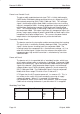
Booster Kit BSH–1 After Sales Technical Documentation DC Characteristics Supply Voltages and Power Consumption Signal Min, Type Max. Unit Notes +12V 1.0 1.2 1.5 A dc +8V 20 25 30 mA dc +5V 5 7 10 mA dc Maximum P Power Level Control Signals Signal Pin TXC X500/23 TX power level control. HP control of booster gain. Value is fed to booster by PWM signal.
After Sales Booster Kit BSH–1 Technical Documentation Power Levels P0 34.5 dBm / 2.82 W P1 30.5 dBm / 1.12 W P2 26.5 dBm / 0.45 W P3 22.5 dBm / 0.18 W P4 18.5 dBm / 71 mW P5 14.5 dBm / 28 mW P6 10.5 dBm / 11 mW P7 6.5 dBm / 4.
Booster Kit BSH–1 After Sales Technical Documentation VC Booster Enable Type dc voltage Level PWR ON PWR OFF 7V to 12V 0V to 1V Load impedance >10k RX Branch from X100 to X101 Frequency range 917 to 950MHz Gain ( typical) 6dB Gain (minimum) 3.5dB Noise Figure (typical) 5 dB Functional description General When the HF Junction box (HFJ) is connected and operational its output line designated VC (+12 V d.c.) provides the power_on command to the RF booster. The booster operates as follows.
After Sales Booster Kit BSH–1 Technical Documentation I/O Map EEPROM Contents The first sixteen (16) bytes carry the RF booster identification part (text string ” RF booster 1.0 ”), the next ten (10) bytes carry power level compensation values and the last ten (10) bytes, RSSI compensation values. When HFJ wants to read the contents of EEPROM, it has to disable the HOOK/SDA and TXI/SCL lines first. After 10 ms, read operation the lines will be back to normal.
Booster Kit BSH–1 After Sales Technical Documentation Power Level Control Circuit The pulse–width modulated control signal TXC is initially fed through a CMOS buffer D300 before being converted into a d.c. voltage by an RC filter network comprising R301, R302, C300 and C301. This analogue signal is fed through rectifier diode V603, and then to the non–inverting input of a comparator N300.
After Sales Booster Kit BSH–1 Technical Documentation Supply Voltage Circuits The supply from the vehicle battery is applied to connector X500. The voltage is first fed through a fuse, followed by suppressor V212 which protects the booster from overvoltages and transients. The voltage is then fed through a filter (L210, C213) eliminating potential interference generated by a vehicle’s electrical system (e.g. alternator).
Booster Kit BSH–1 After Sales Technical Documentation Figure 1: Block Diagram Page 12 Original, 09/94
After Sales Booster Kit BSH–1 Technical Documentation Figure 2: Component Layout Diagram (side 1) Version 05 Original, 09/94 9853883 Page 13
Booster Kit BSH–1 After Sales Technical Documentation Figure 3: Component Layout Diagram (side 2) Version 05 Page 14 9853883 Original, 09/94
After Sales Booster Kit BSH–1 Technical Documentation Parts List 6E 0200100 ITEM CODE DESCRIPTION VALUE TYPE R201 R202 R200 R203 R505 R506 R507 R206 R104 R521 R103 R105 R304 R500 R527 R101 R528 R313 R508 R212 R217 R300 R307 R400 R403 R408 R502 R504 R516 R517 R519 R520 R523 R524 R503 R525 R534 R301 1411388 1411429 1411490 1411490 1411684 1411684 1411684 1412198 1412208 1412303 1412310 1412310 1412335 1412335 1412409 1412416 1412416 1412423 1412423 1412430 1412430 1412430 1412430 1412430 1412430 14
Booster Kit BSH–1 After Sales Technical Documentation ITEM CODE DESCRIPTION VALUE TYPE R302 R410 R533 R308 R501 R207 R216 R310 R311 R312 R401 R402 R409 R512 R513 R514 R530 R531 R522 R526 R511 R102 R314 R518 R205 R509 R208 R309 R100 R204 C300 C301 C603 C200 C201 C205 C206 C610 C100 C101 1412511 1412536 1412536 1412729 1412729 1413635 1413635 1413635 1413635 1413635 1413635 1413635 1413635 1413635 1413635 1413635 1413635 1413635 1413642 1413709 1413804 1413924 1413924 1414011 1414029 1414029 1414036 1
After Sales Booster Kit BSH–1 Technical Documentation ITEM CODE DESCRIPTION VALUE TYPE R201 R202 R200 R203 R505 R506 R507 R206 R104 R521 R103 R105 R304 R500 R527 R101 R528 R313 R508 R212 R217 R300 R307 R400 R403 R408 R502 R504 R516 R517 R519 R520 R523 R524 R503 R525 R534 R301 R302 R410 R308 R501 R533 R207 1411388 1411429 1411490 1411490 1411684 1411684 1411684 1412198 1412208 1412303 1412310 1412310 1412335 1412335 1412409 1412416 1412416 1412423 1412423 1412430 1412430 1412430 1412430 1412430 1412
Booster Kit BSH–1 After Sales Technical Documentation ITEM CODE DESCRIPTION VALUE TYPE R216 R310 R311 R312 R401 R402 R409 R512 R513 R514 R530 R531 R522 R526 R511 R102 R314 R518 R205 R509 R208 R309 R100 R204 C300 C301 C603 C200 C201 C205 C206 C610 C100 C101 C102 C104 C105 C106 C302 C500 C609 C202 C203 C502 C306 C501 1413635 1413635 1413635 1413635 1413635 1413635 1413635 1413635 1413635 1413635 1413635 1413635 1413642 1413709 1413804 1413924 1413924 1414011 1414029 1414029 1414036 1414036 1414043 141
After Sales Booster Kit BSH–1 Technical Documentation ITEM CODE DESCRIPTION VALUE C503 C520 C213 C216 C204 C303 C400 C401 C607 C608 C606 C604 C605 L201 L210 L200 V212 V200 V201 V603 V506 V507 V215 V503 V504 V505 V602 V214 V219 V202 2310791 2310791 2501605 2503803 2604110 2604209 2604209 2604209 2604209 2604209 2604287 2604431 2604431 3606921 3607898 3608206 4100218 4100567 4100567 4100567 4106769 4106769 4107027 4108639 4108639 4108639 4108639 4200603 4200836 4200909 Ceramic cap. Ceramic cap.
Booster Kit BSH–1 After Sales Technical Documentation ITEM CODE DESCRIPTION Z105 Z102 Z101 X100 X101 X500 4508232 4508360 4508362 5422636 5422636 5432120 7313201 9853883 Duplexer ETACS Hz–6/t33/rx–filter 917–950 M ETACS Hz–6/t33/tx–filter 872–905 M ETACS Coaxial connector SFL d=2.5 50 $ pcb Coaxial connector SFL d=2.5 50 $ pcb D25–conn angle m metal bracket UNC Tape pad, white 1x12x25 mm 2–sided PC board BB5 117.5x152.5x1.
After Sales Booster Kit BSH–1 Technical Documentation Figure 4: Exploded View Assembly Parts ITEM 1 2 3 4 5 6 Q’TY CODE 2 24 9537013 9537014 9780014 6150348 6500202 6430144 7 8 9 10 11 C1 Original, 09/94 DESCRIPTION Chassis Cover Antenna cable Screw FeZn Insulating cool pad Plastic rivet 4.0x3.0 socket 6.
Booster Kit BSH–1 After Sales Technical Documentation [This page intentionally left blank] Page 22 Original, 09/94