
User Guide


After Sales
Technical Documentation
Booster Kit BSH–1
Original, 09/94Page 8
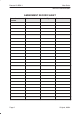
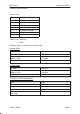
VC Booster Enable
Type dc voltage
Level PWR ON
PWR OFF
7V to 12V
0V to 1V
Load impedance >10k
RX Branch from X100 to X101
Frequency range 917 to 950MHz
Gain ( typical) 6dB
Gain (minimum) 3.5dB
Noise Figure (typical) 5 dB
Functional description
General
When the HF Junction box (HFJ) is connected and operational its output
line designated VC (+12 V d.c.) provides the power_on command to the
RF booster. The booster operates as follows.
HFJ and Booster
After the HFJ is turned on, it first checks whether the booster is connected
or not. This is done by reading the contents of the assumed booster
EEPROM. If the EEPROM contents identification part is recognized, the
HFJ sends an initialization message which indicates to the phone that the
HFJ and the booster are connected. The RSSI and power level
compensation values are also sent, together with the initialization
message. Following the initialization message, the HFJ reads the
TXI/SCL line after a set time period.
Booster
Before the power_on command is enabled, only the mains power switch is
operational. When the booster receives the power_on command, operation
is as follows – the mains power switch starts to conduct and +12 V is fed to
the +8 V regulator. The booster is ready for normal operation. Incoming TXC
(transmitter control, PWM) is initially fed through a CMOS Buffer D300 and
then converted to a d.c. level. This d.c. level is fed to a comparator/driver
which forms part of the RF amplifier feedback loop. The comparator/driver
controls the gain of the RF amplifier.
High RF output at low RF input, or vice versa, signifies a malfunction.
Mains power will be turned off by HFJ; mains power will be turned on
again only if the power_on command is repeated (low to high edge
transition).