3URJUDPPHV $IWHU 0DUNHW 6HUYLFHV 1+0 Q[ Q\ 6HULHV 7UDQVFHLYHUV 7URXEOHVKRRWLQJ ,VVXH $SULO 1RNLD &RUSRUDWLRQ
NHM-2/5nx,ny/6/9 Troubleshooting PAMS Technical Documentation 7DEOH RI &RQWHQWV 3DJH 1R &RPSRQHQW ,GHQWLILFDWLRQ 'LVSOD\ 0RGXOH 6XSSOLHUV 3RJR 3LQ 6XSSOLHUV
NHM-2/5nx,ny/6/9 Troubleshooting PAMS Technical Documentation &RPSRQHQW ,GHQWLILFDWLRQ 1+0 Q[ Q\ XWLOLVH GLIIHUHQW FRPSRQHQW EUDQGV 1RQH RI WKH FRPSRQHQWV PXVW EH VXEVWLWXWHG E\ RWKHU EUDQGV DV LW ZLOO FDXVH PLVDOLJQ PHQW LQ WKH SKRQH 7KH IROORZLQJ NH\ FRPSRQHQWV ZLOO EH VRXUFHG E\ XS WR WKUHH GLIIHUHQW YHQGRUV %HORZ LV D OLVW ZLWK SKRWRV WKDW ZLOO KHOS LGHQWLI\ ZKDW EUDQG RI FRPSRQHQW KDV EHHQ XVHG LQ WKH SKRQH &RPSRQHQW 5HIHUHQFH 9HQGRU 9HQGRU 9HQGRU 3$ 5HI 1 +,7$&+, 3
NHM-2/5nx,ny/6/9 Troubleshooting PAMS Technical Documentation 5HI 1 5)0' 3$ 5HI * 9&7&;2 1'.
NHM-2/5nx,ny/6/9 Troubleshooting PAMS Technical Documentation 5HI = = 'XDO 5; 6$: 3DQDVRQLF 5HI = (*60 7; 6$: (3&26 5HI = (*60 7; 6$: 3DQDVRQLF 5HI ' )/$6+ ,17(/ 5HI ' )/$6+ 67 ,VVXH $SULO 1RNLD &RUSRUDWLRQ 3DJH
NHM-2/5nx,ny/6/9 Troubleshooting PAMS Technical Documentation 5HI = *60 7; 6$: 3DQDVRQLF 5HI = *60 7; 6$: )XMLWVX 5HI * 9&2 )'.
NHM-2/5nx,ny/6/9 Troubleshooting PAMS Technical Documentation 'LVSOD\ 0RGXOH 6XSSOLHUV 7KH HDVLHVW ZD\ WR GHWHUPLQH WKH VXSSOLHU RI WKH GLVSOD\ PRGXOH LV E\ ORRNLQJ DW WKH FRQ QHFWRU DQG FRQQHFWRU FDYLW\ IURP WKH EDFNVLGH RI WKH PRGXOH 3KLOLSV 3KLOLSV GLVSOD\ PRGXOH KDV ODUJH ¦7§ VKDSHG FRQQHFWRU DQG ODUJH FRQQHFWRU FDYLW\ 6HLNR (SVRQ 6HNR (SVRQ GLVSOD\ PRGXOHV KDV VPDOO VTXDUH FRQQHFWRU DQG VPDOO VTXDUH FRQQHFWRU FDYLW\ 3RJR 3LQ 6XSSOLHUV Yokowo PRECI-DIP IMS ø0,09 ±0.03 ø1,02 ±0.02 ø1,08 ±0.
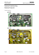
NHM-2/5nx,ny/6/9 Troubleshooting PAMS Technical Documentation %DVHEDQG 7URXEOHVKRRWLQJ %DVHEDQG 7HVWSRLQWV 7RSVLGH &RPSRQHQWV XE & & & / & & & & 5 5 5 5 & - - & - - & - XE & & & 5 & & & & 5 5 5 5 & - - & - - & - 3DJH 1RNLD &RUSRUDWLRQ ,VVXH $SULO
NHM-2/5nx,ny/6/9 Troubleshooting PAMS Technical Documentation XE & & & 5 & 5 5 & & 5 & 5 & - - & - & - - %RWWRP 6LGH &RPSRQHQWV XE XE XE 5 5 & & ,VVXH $SULO 1RNLD &RUSRUDWLRQ 3DJH
NHM-2/5nx,ny/6/9 Troubleshooting PAMS Technical Documentation XE & & & 5 & & & 5 5 & & 5 5 - & - - & - 5 - 5 & 7HVWSRLQW 1HW 1DPH &RQGLWLRQ '& OHYHO $& OHYHO *HQHUDO 5 933 )ODVK RU PXODWHG ((3520 ZULWH 1RPLQDO 9 PLQ 9 PD[ 9 - &&217&6; $FWLYH 6WDWH 3XOVHG DFWLYH 9 QRUPDO VWDWH 9 5 385; 3RZHU XS GRZQ 5HVHW VWDWH 9 1RUPDO VWDWH 9 5 3:521 3:521; :'',6; 3RZHU RQ
NHM-2/5nx,ny/6/9 Troubleshooting PAMS Technical Documentation 7HVWSRLQW 1HW 1DPH &RQGLWLRQ '& OHYHO 5 96<1B 9&26 5) $FWLYH VWDWH 9 PLQ 9 PD[ 9 & 96<1B 9V\QWH 5) $FWLYH VWDWH 9 PLQ 9 PD[ 9 & 97; 9PRG 5) $FWLYH VWDWH 9 PLQ 9 PD[ 9 & 9%% $FWLYH VWDWH 9 PLQ 9 PD[ 9 & 9&2%%$ $FWLYH VWDWH 9 PLQ 9 PD[ 9 & 9&3 $FWLYH VWDWH 1RPLQDO 9 PLQ 9 PD[ 9 & 96,0 $FWLYH VWDWH 1RPLQDO 9 9 6,0 FDUG R
NHM-2/5nx,ny/6/9 Troubleshooting PAMS Technical Documentation 3RZHU 6FKHPDWLF 7HVWSRLQWV - & & & & & & 5 & 5 & & & 3DJH & 1RNLD &RUSRUDWLRQ ,VVXH $SULO
NHM-2/5nx,ny/6/9 Troubleshooting PAMS Technical Documentation 3RZHU 6FKHPDWLF 3ORWV 6\VWHP 3RZHU RQ 3:521; 5 5)& & 385; 5 9;2 & 6\VWHP VOHHS FORFN )UHTXHQF\ LV .+] & ,VVXH $SULO 1RNLD &RUSRUDWLRQ 6/((3&/.
NHM-2/5nx,ny/6/9 Troubleshooting PAMS Technical Documentation &SX 6FKHPDWLF 7HVWSRLQWV 5 5 & - - - 5 5 - 5 3DJH 1RNLD &RUSRUDWLRQ ,VVXH $SULO
NHM-2/5nx,ny/6/9 Troubleshooting PAMS Technical Documentation &38 6FKHPDWLF 3ORWV 6\VWHP FORFN )UHTXHQF\ LV 0+] 5)& & &REED FORFN )UHTXHQF\ LV 0+] - &2%%$&/.
NHM-2/5nx,ny/6/9 Troubleshooting PAMS Technical Documentation )DXOW )LQGLQJ &KDUWV 3KRQH LV 'HDG 3KRQH LV GHDG PHDQV WKDW WKH SKRQH GRHV QRW WDNH FXUUHQW ZKHQ WKH SRZHU VZLWFK LV SUHVVHG RU ZKHQ WKH ZDWFKGRJ GLVDEOH SLQ :'',6; LV JURXQGHG 1RPLQDO VXSSO\ YROWDJH WR WKH SKRQH LV 9 9EDW YROWDJH ,I WKH EDWWHU\ YROWDJH LV EHORZ 9 WKH &&217 SUH YHQWV WKH SKRQH IURP SRZHULQJ XS The phone is dead The voltage at C404, C202, C226, C227, C228 is = 3,6V No Failiure in Vbatt line.
NHM-2/5nx,ny/6/9 Troubleshooting PAMS Technical Documentation Because of the use of ìBGA components it is not possible to verify if there is a short-circuit in any of the lines to and from the MAD2WD1 and the SRAM/flash circuits. The fault finding diagrams for flash programming are as follows.
NHM-2/5nx,ny/6/9 Troubleshooting PAMS Technical Documentation )ODVK SURJUDPPLQJ GLDJUDP Flash programming doesn’t work External RAM error Yes Check for activity on control lines for SRAM : J323 (RAMSelX) Yes Defective SRAM (D302) No Defective MAD2 (D300) or short circuit under the SRAM No Algorithm file or alias not found.
NHM-2/5nx,ny/6/9 Troubleshooting PAMS Technical Documentation )ODVK H[FKDQJH SURFHGXUH 7R FKDQJH ' EDFNXS WKH RSKRQH LGHQWLW\ LQIRUPDWLRQ E\ XVLQJ :LQ7HVOD 2SHQ XQGHU 9LHZ WKH ZLQGRZ 3KRQH ,QIRUPDWLRQ ,I \RX FDQQRW VDYH WKLV GDWD H J SKRQH GRHV QRW VZLWFK RQ EHFDXVH RI GHIHFW ' LW LV QHFHVVDU\ WR JLYH WKH SKRQH D QHZ LGHQWLW\ ,I \RX KDYH VDYHG WKH SKRQH LGHQWLW\ LQIRUPDWLRQ \RX FDQ QRZ UHPRYH ' DQG UHVROGHU WKH VSDUHSDUW DOZD\V XVH DSSURYHG µ%*$ UHZRUN PDFKLQH IRU FKDQJLQJ DQ\ µ%*$
NHM-2/5nx,ny/6/9 Troubleshooting PAMS Technical Documentation 1RZ \RX KDYH FKRVHQ D 0&8 ,PDJH )LOH DQG 330 )LOH IRU \RXU SKRQH E\ SUHVVLQJ RQ WKH VTXDUHV ZLWK WKH WKUHH GRWV $W WKLV SRLQW LW LV QRW QHFHVVDU\ WR FKRRVH WKH ULJKW ILOH EHFDXVH WKLV 6: XSGDWH LV XVHG RQO\ WR PDNH LW SRVVLEOH WR SRZHU WKH SKRQH RQ $IWHU VHOHFWLQJ WKH WZR ILOHV \RX KDYH WR SUHVV WKH )ODVK EXWWRQ WR VWDUW WKH 6: XSGDWH 1H[W PHVVDJH ZLOO EH WKH IROORZLQJ 6HOHFW
NHM-2/5nx,ny/6/9 Troubleshooting PAMS Technical Documentation 1H[W PHVVDJH \RX ZLOO JHW LV WKLV $IWHU SUHVVLQJ
NHM-2/5nx,ny/6/9 Troubleshooting PAMS Technical Documentation 5HPHPEHU WR UHWXQH 5; 7; YDOXHV DQG UXQ HQHUJ\ PDQDJHPHQW FDOLEUDWLRQ EHFDXVH DOO WXQLQJ GDWD LV ORVW DIWHU FKDQJLQJ ' 3KRQH 6WD\V 2Q RU LV -DPPHG ,I WKLV NLQG RI HUURU RFFXUV DIWHU IODVKLQJ WKH PRVW SODXVLEOH UHDVRQ LV RSHQ SLQV RQ DQ ,& 1RUPDOO\ WKH &&217 ZLOO SRZHU WKH SKRQH GRZQ DIWHU VHFRQGV LI WKH ZDWFKGRJ KDV QRW EHHQ VHUYHG E\ 6: &RQQHFWLQJ DQ RVFLOORVFRSH WR - 'DWD6HO; RQ WKH &&217 FDQ PRQLWRU WKH ZDWFKGRJ XSGDWLQJ
NHM-2/5nx,ny/6/9 Troubleshooting PAMS Technical Documentation 'LVSOD\ ,QIRUPDWLRQ ¦&RQWDFW 6HUYLFH§ ,I WKH PHVVDJH &RQWDFW 6HUYLFH LV GLVSOD\HG RQH RU PRUH SDUWV RI WKH VRIWZDUH LV XQDEOH WR H[HFXWH SURSHUO\ $W WKH VDPH WLPH WKH ZDWFKGRJ LV WULJJHUHG DQG LV WKHUHE\ DEOH WR WHOO LI DQ HUURU KDV RFFXUUHG 6HOIWHVW IXQFWLRQV DUH H[HFXWHG ZKHQ WKH SKRQH LV SRZHUHG RQ DQG LI RQH RU PRUH VHOIWHVW IXQFWLRQV IDLOV WKH PHVVDJH &RQWDFW 6HUYLFH LV VKRZQ LQ WKH GLVSOD\ 0&8 VHOIWHVW FDVHV FDQ EH VSOLW LQ
NHM-2/5nx,ny/6/9 Troubleshooting PAMS Technical Documentation 1R 1HWZRUN )RXQG 1R &DOO (VWDEOLVKHG :KHQ WKH SKRQH LV XQDEOH WR HLWKHU ILQG D QHWZRUN RU HVWDEOLVK D FDOO ERWK WKH 5) SDUW DQG WKH EDVHEDQG SDUW FDQ FDXVH LW 7KH SKRQH FDQ EH VHW WR UHTXLUHG PRGH 5) PHDVXUH PHQWV E\ WKH :LQ7HVOD VHUYLFH VRIWZDUH LQ RUGHU WR GHWHUPLQH LI WKH HUURU LV SODFHG HLWKHU LQ WKH 5) SDUW RU WKH EDVHEDQG SDUW 7KHUH DUH WZR FLUFXLWV WKDW VXSSOLHV WKH 5) SDUW RI WKH SKRQH 7KHVH FLUFXLWV DUH 0$' :' ' &2%%$
NHM-2/5nx,ny/6/9 Troubleshooting PAMS Technical Documentation 3KRQH 1RW 5HJLVWHLQJ WR D 1HWZRUN Phone doesn’t register to a network or the phone is unable to make a call C207 (Vcobba) > 2,7V No Check CCONT (N201) Yes Vref at C201 =1,5V Check C210, R509 and C536.
NHM-2/5nx,ny/6/9 Troubleshooting PAMS Technical Documentation 6LP 5HODWHG (UURUV 7KH 6,0 LQWHUIDFH IURP WKH 0$' :' ' WR WKH 6,0 FRQQHFWRU ; FDQ EH WHVWHG ZLWKRXW D 6,0 FDUG :KHQ WKH SRZHU LV VZLWFKHG RQ DQG WKH %6, WHUPLQDO LV JURXQGHG E\ D UHVLVWRU DOO LQWHUIDFH OLQHV 96,0 '$7$B$ 6,0567B$ 6,0&/.
NHM-2/5nx,ny/6/9 Troubleshooting PAMS Technical Documentation 6,0 FDUG UHMHFWHG HUURU "SIM card rejected" Vsim according to spec.: 2,8V min. (3V SIM card) 4,5V min.
NHM-2/5nx,ny/6/9 Troubleshooting PAMS Technical Documentation ,QWHUQDO PLFURSKRQH Microphone doesn’t work and there aren’t any electrical or mechanical problems. C115 towards R115 (bias) = 2,1V No Check R115, V101, C123, C113. Yes Check mic-line to COBBA : L402, C403, C407, C120, R111. OK Replace COBBA (N100) ([WHUQDO HDUSHDFH Headset earpiece doesn’t work and there are no mechanical problems Check L401, R109, C101, C107. OK Replace COBBA (N100).
NHM-2/5nx,ny/6/9 Troubleshooting PAMS Technical Documentation &KDUJLQJ (UURU 1R GHWHFWLRQ RI FKDUJHU Nothing happens when a charger is connected to the phone Yes The voltage at R210 towards R209 > 0,4V No Check F200, L202, R209, R210 Yes Replace CCONT (N201) ¦1RW &KDUJLQJ§ PHVVDJH "Not charging" message appears in the display Yes The voltage at R220 towards C236 (BSI, N201) = 0,8V when a charger is connected.
NHM-2/5nx,ny/6/9 Troubleshooting PAMS Technical Documentation 5) 7URXEOHVKRRWLQJ 7ZR W\SHV RI PHDVXUHPHQWV DUH XVHG LQ WKH IROORZLQJ ,W ZLOO EH VSHFLILHG LI WKH PHDVXUHPHQW W\SH LV 5) RU /) 5) PHDVXUHPHQWV VKRXOG EH GRQH ZLWK D 6SHFWUXP $QDO\]HU DQG D KLJK IUH TXHQF\ RKP SDVVLYH SUREH IRU H[DPSOH +3 $ 1RWH WKDW ZKHQ PHD VXULQJ ZLWK WKH RKP SUREH WKH VLJQDO ZLOO EH DURXQG G% DWWHQXDWHG 7KH YDOXHV LQ WKH IROORZLQJ ZLOO KDYH WKHVH G% VXEWUDFWHG DQG UHSUHVHQW WKH UHDO YD
NHM-2/5nx,ny/6/9 Troubleshooting PAMS Technical Documentation 5) .
NHM-2/5nx,ny/6/9 Troubleshooting PAMS Technical Documentation 1 3RZHU DPSOLILHU 3$ = 5;7; VZLWFK = VW 'XDO 5; 6$: ILOWHU (*60 *60 = QG 'XDO 5; 6$: ILOWHU (*60 *60 * 9&7&;2 0+] &U\VWDO RVFLOODWRU 1 +DJDU 5) ,& * 9&2 *+] 8+) 9&2 = (*60 7; 6$: ILOWHU *60 = *60 7; 6$: ILOWHU RQO\ PRGXOH 8' 8; $EEUHYLDWLRQV LQ )DXOW )LQGLQJ &KDUWV 3DJH %% %DVHEDQG '& 'LUHFW &XUUHQW (6' (OHFWUR 6WDWLF 'LFKDUJH I )UHTXHQF\ RI VLJQDO
NHM-2/5nx,ny/6/9 Troubleshooting PAMS Technical Documentation 5; 7URXEOHVKRRWLQJ 8VH FKDUW EHORZ DV HQWU\ SRLQW IRU JHQHUDO 5; WURXEOHVKRRWLQJ Set to Local Mode Band = don’t care RX Burst mode Channel = don’t care RX troubleshooting Apply NO signal to antenna connector Measure RXI and RXQ with oscilloscope (500mV/div, 500us/div) Both signals looks like Figure 1 (Note 1+2) Yes RX chain functional Local Burst mode Go to EGSM RX Troubleshooting chart No One or both signals looks like Figure 2 or Y
NHM-2/5nx,ny/6/9 Troubleshooting PAMS Technical Documentation Figure 1 I/Q working ok 3DJH 1RNLD &RUSRUDWLRQ ,VVXH $SULO
NHM-2/5nx,ny/6/9 Troubleshooting PAMS Technical Documentation Figure 2 Check C508 ,VVXH $SULO 1RNLD &RUSRUDWLRQ 3DJH
NHM-2/5nx,ny/6/9 Troubleshooting PAMS Technical Documentation Figure 3 Check C508+ C515 3DJH 1RNLD &RUSRUDWLRQ ,VVXH $SULO
NHM-2/5nx,ny/6/9 Troubleshooting PAMS Technical Documentation Figure 4 Check C508 ,VVXH $SULO 1RNLD &RUSRUDWLRQ 3DJH
NHM-2/5nx,ny/6/9 Troubleshooting PAMS Technical Documentation Figure 5 Check C512 3DJH 1RNLD &RUSRUDWLRQ ,VVXH $SULO
NHM-2/5nx,ny/6/9 Troubleshooting PAMS Technical Documentation Figure 6 Check C514 ,VVXH $SULO 1RNLD &RUSRUDWLRQ 3DJH
NHM-2/5nx,ny/6/9 Troubleshooting PAMS Technical Documentation Figure 7 Check C526 3DJH 1RNLD &RUSRUDWLRQ ,VVXH $SULO
NHM-2/5nx,ny/6/9 Troubleshooting PAMS Technical Documentation (*60 5HFHLYHU 7URXEOHVKRRWLQJ 5[ PHDVXUHPHQW SRLQWV XE B XE B XE B Rx/Tx switch, EGSM_Rx C556 GSM1800 LNA, RF out C519 LNA_P, GSM1800 C568 GSM 1800 LNA, RF in L505 1st Rx SAW, GSM1800 out Z501 Rx/Tx swicth, VC1 - Z502 Rx/Tx switch, VC2 - Z502 1st Rx SAW , EGSM out Z501 Rx/Tx switch, ANT - Z502 Rx/Tx switch, DCS_Rx (GSM1800) Z502 Z502 1st Rx SAW 1st Rx SAW, GSM1800 in EGSM in ,VVXH $SULO 1RNLD &RUSRUDWLRQ 3DJH
NHM-2/5nx,ny/6/9 Troubleshooting PAMS Technical Documentation EGSM LNA in - LNA_G, EGSM - V501 C545 LNAB_D, EGSM - R508 2nd Rx SAW GSM1800 in Z500 EGSM LNA out / 2nd Rx SAW, EGSM in - C534 2nd Rx SAW GSM1800 out Z500 2nd Rx SAW, EGSM out Z500 RXIP and RXQP R504 3DJH 1RNLD &RUSRUDWLRQ ,VVXH $SULO
NHM-2/5nx,ny/6/9 Troubleshooting PAMS Technical Documentation Rx measurement points, ub4_10 / ub4_11..
NHM-2/5nx,ny/6/9 Troubleshooting PAMS Technical Documentation EGSM LNA in C545 LNAB_D, EGSM - R508 2nd Rx SAW, GSM1800 in Z500 EGSM LNA out / 2nd Rx SAW, EGSM in - C534 2nd Rx SAW, GSM1800 out Z500 LNA_G, EGSM - R514 RXIP and RXQP R504 2nd Rx SAW, EGSM out Z500 *HQHUDO LQVWUXFWLRQV IRU (*60 5; WURXEOHVKRRWLQJ Connect the phone to a PC with the module repair jig.
NHM-2/5nx,ny/6/9 Troubleshooting PAMS Technical Documentation The set-up should now look like this: Apply a 942.667 MHz (channel 38 + 67.710kHz offset) -55 dBm signal to the RF-connector.
NHM-2/5nx,ny/6/9 Troubleshooting PAMS Technical Documentation )DXOW ILQGLQJ FKDUW IRU (*60 UHFHLYHU Set to Local Mode EGSM RX continuos Channel = 38 AGC abs. = 4 EGSM RX Troubleshooting Apply -55dBm 942.
NHM-2/5nx,ny/6/9 Troubleshooting PAMS Technical Documentation (*60 6LJQDO SDWK For easy error tracing it is important to know the signal path of the EGSM receiver. The components can be grouped into blocks and drawn as shown below.
NHM-2/5nx,ny/6/9 Troubleshooting PAMS Technical Documentation *60 5HFHLYHU 7URXEOHVKRRWLQJ *HQHUDO LQVWUXFWLRQV IRU *60 5; WURXEOHVKRRWLQJ Connect the phone to a PC with the module repair jig. Start Wintesla-Service-Software and Select Product Alt+p Open… NHM-5 Select: Product Alt+p Band b p PCN Select: Testing Alt+e RF Controls r RX Continuous Alt+r Cont. Mode Ch: 700 Alt+o, 700 AGC Absolute: 4 Apply The set-up should now look like this: Apply an 1842.867 MHz (channel 700 + 67.
NHM-2/5nx,ny/6/9 Troubleshooting PAMS Technical Documentation Signal amplitude ~570V DC offset 1,2V Frequency 67kHz If this picture is not seen not go to section Fault finding chart for GSM1800 receiver of this document ,VVXH $SULO 1RNLD &RUSRUDWLRQ 3DJH
NHM-2/5nx,ny/6/9 Troubleshooting PAMS Technical Documentation )DXOW ILQGLQJ FKDUW IRU *60 UHFHLYHU Set to Local Mode PCN RX continuos Channel = 700 AGC abs. = 4 GSM1800 RX Troubleshooting Apply -55dBm 1842.
NHM-2/5nx,ny/6/9 Troubleshooting PAMS Technical Documentation *60 6LJQDO SDWK For easy error tracing it is important to know the signal path of the GSM1800 receiver. The components can be grouped into blocks and drawn as shown below.
NHM-2/5nx,ny/6/9 Troubleshooting PAMS Technical Documentation The signal-path is through Z501 (In-band insertion-loss 3,5dB), through the matching circuit (C517 ) and to the GSM1800 LNA (V500, RFin). The LNA has about 18dB gain when it is "on" (LNAB_G = 2.8V and LNA_P = 0V). If the signal applied to the antenna-connector is more than –45dBm the AGC will gain-step the LNA (LNAB_G = 2.8V and LNA_P = 0V) which means the LNA Gain will now have negative gain (loss) of –12dB.
NHM-2/5nx,ny/6/9 Troubleshooting PAMS Technical Documentation 5; 1RUPDO 0RGH 7URXEOHVKRRWLQJ After any repair, reflash, retuning etc. the receiver performance must be checked in normal mode. Place phone PWB in module repair jig or use service battery and antenna adapter, follow instructions in chart in chart below: Connect Phone to GSM tester, and set to Normal mode RX troubleshooting Normal mode Wait for Service indicator, Setup call.
NHM-2/5nx,ny/6/9 Troubleshooting PAMS Technical Documentation (*60 7UDQVPLWWHU V_ANT_1/ V_ANT_2 RF Controls 2 VB_DET VTXLO_G RX Ant Switch PCN TX RX OUTP_D_TX/ OUTM_D_TX GSM 2 TX OUTP_G_TX/ OUTM_G_TX PA Dir.
NHM-2/5nx,ny/6/9 Troubleshooting PAMS Technical Documentation 7; PHDVXUHPHQW SRLQWV XE XE Rx/Tx switch, VC2 - Z502 Rx/Tx switch, VC1 - Z502 DET0 - C588 Rx/Tx switch, ANT - Z502 Rx/Tx switch, DCS_Tx (GSM1800) - C569 Rx/Tx switch, EGSM_Tx - L518 PA, Pout GSM1800 N502 Antenna pad PA, Pout EGSM - N502 PA, Vtxlo - N502 PA, Vpctrl EGSM - R532 PA, Pin GSM1800 - N502 PA, Pin EGSM R551 PA, Vpctrl GSM1800 - N502 TXI and TXQ R541 and R548 T503 unbalanced C566 T504 unbalanced ,VVXH $SULO
NHM-2/5nx,ny/6/9 Troubleshooting PAMS Technical Documentation 7; PHDVXUHPHQW SRLQWV XE XE XE Rx/Tx switch, VC2 - Z502 Rx/Tx switch, VC1 - Z502 Rx/Tx switch, ANT- Z502 Rx/Tx switch, DCS_Tx (GSM1800) - C569 DET0 - C588 Rx/Tx switch, EGSM_Tx - L518 PA, Pout GSM1800 N502 Antenna pad PA, Pout EGSM - N502 PA, Vpctrl EGSM - R532 PA, Pin GSM1800 - N502 N502 PA, Pin EGSM R551 3DJH PA, Vpctrl GSM1800 - N502 1RNLD &RUSRUDWLRQ ,VVXH $SULO
NHM-2/5nx,ny/6/9 Troubleshooting PAMS Technical Documentation T503 unbalanced Z504 or C566 TXI and TXQ R541 and R548 T504 unbalanced *HQHUDO LQVWUXFWLRQV IRU (*60 7; WURXEOHVKRRWLQJ Start WinTesla-Service-Software and Select: Alt+p Product Band b GSM Select: g Testing Alt+e RF Controls ,VVXH $SULO r TX Burst Alt+b TX Data Type: Random Alt+d, r TX Power Level : 5 Alt+x, 5 Channel: 60 Alt+n, 60 Apply Alt+a 1RNLD &RUSRUDWLRQ 3DJH
NHM-2/5nx,ny/6/9 Troubleshooting PAMS Technical Documentation Your screen should look like this: Measure the output power of the phone; it should be around 32 dBm.
NHM-2/5nx,ny/6/9 Troubleshooting PAMS Technical Documentation )DXOW ILQGLQJ FKDUW IRU (*60 WUDQVPLWWHU )DXOW ILQGLQJ LQ RXWSXW SRZHU For the spectrum analyzer measurements in the following chart use the 500 ohm passive probe. Since the signal measured is bursted it is advised to set the analyzer to maxhold. Measure TX power on "ANT" Power > 30.5 dBm in 50 ohm. No Measure TX power on GSM_Tx. Power ~ 8 dBm in 500 ohm No Measure TX power on "Pout". Power ~ 8 dBm in 500 ohm No Measure TX power on "Pin".
NHM-2/5nx,ny/6/9 Troubleshooting PAMS Technical Documentation )DXOW ILQGLQJ LQ PRGXODWLRQ The following plots show different situations of TX IQ measurements. Depending on the time the modulation may cause the signal to look differently. For how to check Hagar and serial bus see section Hagar and serial interface.
NHM-2/5nx,ny/6/9 Troubleshooting PAMS Technical Documentation *60 7UDQVPLWWHU *HQHUDO LQVWUXFWLRQV IRU *60 7; WURXEOHVKRRWLQJ Apply a RF-cable to the RF-connector to allow the transmitted signal act as normal. RF-cable should be connected to measurement equipment or to at least a 10-dB attenuator, otherwise the PA may be damaged.
NHM-2/5nx,ny/6/9 Troubleshooting PAMS Technical Documentation 3DWK RI WKH WUDQVPLWWHG *60 VLJQDO Fault finding chart for GSM1800 transmitter Measure TX power on "ANT" Power > 27.5 dBm in 50 ohm No Measure TX power on DCS_Tx. Power ~7 dBm in 500 ohm No Measure TX power on "Pout". Power ~7 dBm in 500 ohm No Measure TX power on "Pin". Power ~-17 dBm in 500 ohm Yes Yes Yes Yes Check POGO pins, C593, L510 With Osc on RXTX switch check: Vc1 = 2.
NHM-2/5nx,ny/6/9 Troubleshooting PAMS Technical Documentation 0HDVXUHPHQW SRLQWV DW WKH 9&7&;2 9&7&;2 PHDVXUHPHQW SRLQWV XE B XE B VCTCXO, Vtcxo (2.7V) C543 VCTCXO, buffer input - V502 VCTCXO, 26 MHz out C546 RFC, 13MHz L511 9&7&;2 PHDVXUHPHQW SRLQWV XE B XE B DQG XE B VCTCXO, Vtcxo (2.
NHM-2/5nx,ny/6/9 Troubleshooting PAMS Technical Documentation 9&2 PHDVXUHPHQW SRLQWV XE B XE B T502 unbalanced VCOS - R202 *HQHUDO LQVWUXFWLRQV IRU 6\QWKHVL]HU WURXEOHVKRRWLQJ Start WinTesla-Service-Software and Select: Product Alt+p b Band EGSM Select: e Testing Alt+e RF Controls r RX Continuous Alt+r Cont. Mode Ch: 60 Alt+o, 60 Measure the output of the VCO (G500) at T502 with spectrum analyzer and 500 ohm passive probe; the power should be around –20 dBm.
NHM-2/5nx,ny/6/9 Troubleshooting PAMS Technical Documentation COBBA. Range of Vcon is 0.3 – 2.3 V.
NHM-2/5nx,ny/6/9 Troubleshooting PAMS Technical Documentation 9&2 The VCO is generating frequencies in the range of 3420 – 3840 MHz when PLL is in function. These are divided by 2 or by 4 in HAGAR so that they can generate all channels in EGSM and GSM1800. Frequency of the VCO is controlled by dc voltage ( Vc ) coming from the loop filter. Range of the Vc when PLL is in function is 0.7 – 3.8 V.
NHM-2/5nx,ny/6/9 Troubleshooting PAMS Technical Documentation If the phone gets ‘dead’ very short time after the power is turned ON, possible reason for this might be that 13 MHz system clock signal is not coming to the BB. Use the following chart to find the problem. Oscilloscope Oscilloscope Turn the phone ON and measure VCTCXO (G502) power supply Vtcxo at C543 - 2,7 V No Check CCONT, phone is ’dead’ Yes Oscilloscope Measure 26 MHz VCTCXO output signal at C546 - approx. 1.2 Vpp.
NHM-2/5nx,ny/6/9 Troubleshooting PAMS Technical Documentation )UHTXHQF\ OLVWV (*60 )UHTXHQF\ OLVW 1+0 (*60 Frequency list NHM-5 GSM900 CH TX RX VCO TX VCO RX 975 880.2 925.2 3520.8 3700.8 976 880.4 925.4 3521.6 3701.6 977 880.6 925.6 3522.4 3702.4 978 880.8 925.8 3523.2 3703.2 979 881 926 3524 3704 980 881.2 926.2 3524.8 3704.8 981 881.4 926.4 3525.6 3705.6 982 881.6 926.6 3526.4 3706.4 983 881.8 926.8 3527.2 3707.2 984 882 927 3528 3708 985 882.2 927.2 3528.8 3708.8 986 882.4 927.4 3529.6 3709.
NHM-2/5nx,ny/6/9 Troubleshooting PAMS Technical Documentation *60 CH 512 513 514 515 516 517 518 519 520 521 522 523 524 525 526 527 528 529 530 531 532 533 534 535 536 537 538 539 540 541 542 543 544 545 546 547 548 549 550 551 552 553 554 555 556 557 558 559 560 561 562 563 564 565 565 566 567 568 569 570 571 572 573 574 575 576 577 578 579 580 581 582 583 584 585 586 587 588 589 590 591 592 593 594 595 596 597 598 599 600 601 602 603 604 605 TX 1710,2 1710,4 1710,6 1710,8 1711 1711,2 1711,4 1711,6
NHM-2/5nx,ny/6/9 Troubleshooting PAMS Technical Documentation +DJDU DQG VHULDO LQWHUIDFH In general, if phone is not in a sleep mode, Hagar chip is always active. This means that, as long as we have set the phone in Normal mode or in Local mode (either RX or TX band ) there is going to be some Hagar activities, which is controled through serial interface (SDATA,SCLK,SENA and HAGAR_RESET_X).
NHM-2/5nx,ny/6/9 Troubleshooting PAMS Technical Documentation First precondition for Hagar to be in active (ON) mode is that HAGAR_RESET_X should be high (2.8V) and VREF, which is Hagar reference voltage, at 1.35V. Easiest way to check these two voltages is by using oscilloscope with an standard passive probe (10kΩ/8pF). HAGAR_RESET_X is measured on C540 and VREF on C536. Another " good spot" to check if Hagar’s internal supplies are active, is to measure either on capacitor C538 or resistor R511.
NHM-2/5nx,ny/6/9 Troubleshooting PAMS Technical Documentation :LQWHVOD 7XQLQJ Prior to any tuning the phone should be initialised: Start Wintesla-Service-Software and Select Alt+p Product Open… NHM-5 Select: Alt+p Product Initialise Alt+I Normal Mode F5 :KDW 5) WR WXQH DIWHU UHSDLUV Different repairs require different tuning. In general it is necessary to determine in which section the repair was done to establish which tunings to perform.
NHM-2/5nx,ny/6/9 Troubleshooting PAMS Technical Documentation 5; &DOLEUDWLRQ The "RX calibration" is used to determine gain at different gain-settings for front-end and Hagar and needs to be done in both bands, but the calibration only have to be started once, it will automatically proceed to the GSM1800 band after EGSM.
NHM-2/5nx,ny/6/9 Troubleshooting PAMS Technical Documentation Click OK in the Wintesla window, now a new window pops up: Click Save in the Wintesla window, now a new window pops up: Change the level and frequency on the generator as the window tells you.
NHM-2/5nx,ny/6/9 Troubleshooting PAMS Technical Documentation Change the level and frequency on the generator as the window tells you.
NHM-2/5nx,ny/6/9 Troubleshooting PAMS Technical Documentation 5; )LOWHU &DOLEUDWLRQ $XWRPDWLF This calibration is calibrating the Baseband filter inside Hagar, for this reason the calibration is not done in both bands. Select: Tuning Alt+t RX Measurements A window now pops-up: In the "Select Function" frame select RX "Filter calibration (Automatic)".
NHM-2/5nx,ny/6/9 Troubleshooting PAMS Technical Documentation 5; $0 6XSSUHVVLRQ $XWRPDWLF This calibration is tuning the AM suppression performance of Hagar mixers and will have to be done in both bands. If flash or Hagar has been replaced or Full Factory settings have been performed RX AM Suppression must be done. EGSM Select: Product Alt+p Band b EGSM Select: Tuning e Alt+t RX Measurements A window now pops-up: In the "Select Function" frame select RX "RX AM Suppression (Automatic)".
NHM-2/5nx,ny/6/9 Troubleshooting PAMS Technical Documentation Click OK in the Winteslwindow, the RSSI value is updated in the RX Measurements window. Click "Save ". The "RX AM suppression tuning" is now completed in EGSM. Click “Yes” to proceed to PCN band *60 Select: Product Alt+p Band b PCN Select: Tuning p Alt+t RX Measurements In the "Select Function" frame select RX "RX AM Suppression (Automatic)".
NHM-2/5nx,ny/6/9 Troubleshooting PAMS Technical Documentation Click Measure, A window now pops-up: Connect an external generator to the antenna connector of the phone and set-up the generator. Click OK in the Wintesla window, the RSSI value is updated in the RX Measurements window.
NHM-2/5nx,ny/6/9 Troubleshooting PAMS Technical Documentation Click "Save ". The "RX AM suppression tuning" is now completed in PCN. 7; 3RZHU WXQLQJ This tuning must be done in both bands.
NHM-2/5nx,ny/6/9 Troubleshooting PAMS Technical Documentation A window now pops-up: Tune level 19, 15, 5 and Base in accordance with the target values. Note: Target values may vary due to different PA vendors. Click calculate, check if the other levels match the targets, correct if necessary. Click Save when all values match the targets.
NHM-2/5nx,ny/6/9 Troubleshooting PAMS Technical Documentation *60 Select: Product Alt+p b Band PCN Select: p Testing Alt+e RF Controls r A window now pops-up: Set Active unit to TX Set TX Data Type: to Rand Click Apply Click Close Select: Tuning Alt+t TX Power… 3DJH Alt+P 1RNLD &RUSRUDWLRQ ,VVXH $SULO
NHM-2/5nx,ny/6/9 Troubleshooting PAMS Technical Documentation A window now pops-up: Tune level 15, 11, 0 and Base in accordance with the target values. Note: Target values may vary due to different PA vendors. Click calculate, check if the other levels match the targets, correct if necessary. Click Save when all values match the targets.
NHM-2/5nx,ny/6/9 Troubleshooting PAMS Technical Documentation 7; , 4 7XQLQJ This tuning must be done in both band Initial set-up EGSM Select: Alt+p Product Band b EGSM Select: e Testing Alt+e RF Controls r A window now pops-up: Set Active unit to TX Set TX Data Type: to Cont1 Click Apply Click Close Go through the "Common tuning procedure for EGSM and GSM1800" described in section 11.6.2 of this document.
NHM-2/5nx,ny/6/9 Troubleshooting PAMS Technical Documentation ,QLWLDO VHW XS *60 Select: Product Alt+p b Band PCN Select: p Testing Alt+e RF Controls r A window now pops-up: Set Active unit to TX Set TX Data Type: to Cont1 Click Apply Click Close Go through the "Common tuning procedure for EGSM and GSM1800" described in section 11.6.2 of this document.
NHM-2/5nx,ny/6/9 Troubleshooting PAMS Technical Documentation &RPPRQ WXQLQJ SURFHGXUH IRU (*60 DQG *60 Select: Tuning Alt+t Alt+q TX I/Q… A window now pops-up: The carrier (M2) and +67kHz (M3) signal should now be tuned to a minimum. The buttons in the "TX I and Q DC Offset:" will change the level of the carrier. The buttons in the "Amplitude and Phase Difference:" window will change the level of the +67kHz signal.