PAMS Technical Documentation NPM–9 Series Transceivers Troubleshooting Instructions Issue 1 02/2002 Nokia Corporation
NPM–9 Troubleshooting Instructions PAMS Technical Documentation CONTENTS Transceiver Troubleshooting . . . . . . . . . . . . . . . . . . . . . . . . . . . . . Baseband Troubleshooting . . . . . . . . . . . . . . . . . . . . . . . . . . . . PWB Test Points . . . . . . . . . . . . . . . . . . . . . . . . . . . . . . . . . . . Measurement Points . . . . . . . . . . . . . . . . . . . . . . . . . . . . . . . . Troubleshooting steps . . . . . . . . . . . . . . . . . . . . . . . . . . . . . .
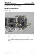
NPM–9 Troubleshooting Instructions PAMS Technical Documentation Transceiver Troubleshooting Baseband Troubleshooting PWB Test Points MBUSTX FBUSRX MBUSRX FBUSTX SLEEPCLK CBUSDA DBUSCLK DBUSDA UEMINT PURX CBUSCLK MBUS VPP DBUSENX1 GND CBUSENX SLEEPX FMCLK FBUSTX FMTUNEX FMCTRLDA FBUSRX FMCTRLCLK FMWREN EXTRDX FPS–8 FM RADIO BLACK colored test points are connected to the lines between UEM and UPP where the logic level is 1.8 V.
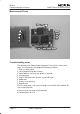
NPM–9 Troubleshooting Instructions PAMS Technical Documentation Measurement Points VR5 2.78 V VR7 2.78 V VR3 2.78 V VOUT VFLASH2 2.78 V VDD 2.78 V VR1B 4.75 V VDDI 1.8 V VR1A 4.75 V SCLK VR2 2.78 V SDA VR6 2.78 V GND VR4 2.78 V XCS XRES VIO 1.8V VCORE 1.8V VANA 2.78 V VFLASH1 2.78 V Troubleshooting steps The following hints help to find the problem if the circuitry seems to be faulty. The instructions are divided into following sections: 1. Phone is totally dead 2.
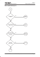
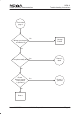
PAMS Technical Documentation NPM–9 Troubleshooting Instructions Main troubleshooting tree TOP Phone totally dead Yes Phone is dead Yes Flash faults No Flash programming doesn’t work No Phone doesn’t Yes start up or the phone is jammed Phone is jammed No Charging doesn’t work Yes Charger No TOP 2 Issue 1 02/2002 Nokia Corporation Page 5
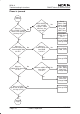
NPM–9 Troubleshooting Instructions PAMS Technical Documentation TOP 2 Phone doesn’t read SIM card Yes SIM card No Yes Audio faults Yes Display faults Yes Keypad faults Audio faults No Display or LED’s doesn’t work No Keypad doesn’t work No END Page 6 Nokia Corporation Issue 1 02/2002
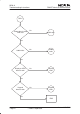
NPM–9 Troubleshooting Instructions PAMS Technical Documentation Phone is dead Phone is dead Phone current is zero ? Check X101 solder and VBATT lines Yes No Yes Phone current is < 50mA No Yes Is phone flash programing OK ? Phone is jammed No Flash faults No Phone current is ~ 54 mA Yes Is phone in LOCAL MODE ? Yes No Check BSI line Yes X101, C241, R203, C109, R202 Are they OK ? Change UEM No Repair OK retest Issue 1 02/2002 Nokia Corporation Page 7
NPM–9 Troubleshooting Instructions PAMS Technical Documentation Flash programming doesn’t work Flash faults The Phone does Yes not set Flashbus TXD line high after the startup. Measure BSI pulse during Flash programming. Is it OK ? No Check BSI line X101, C241, R203, C109, R202 Yes Measure FBUSTX line during Flash programming from testpoint J411 Is it High (1.8V) ? Yes The Phone does not set Flashbus TXD line low after the line has been high.
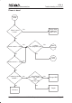
PAMS Technical Documentation NPM–9 Troubleshooting Instructions Flash faults page 2 Yes Change FLASH Yes Is the phone totally dead ? Phone is dead Wrong manufactor ID and Device ID No No Phone doesn’t start up or the phone is jammed ? Yes Phone is jammed No Retest Issue 1 02/2002 Nokia Corporation Page 9
NPM–9 Troubleshooting Instructions PAMS Technical Documentation Phone is jammed Phone is jammed Measure VIO, VCORE, FLASH1, No VANA, VR3 voltages. Are they OK ? Check VBATT1–6 VIO, VCORE, FLASH1, VANA, VR3 lines. Are they OK? No Check BSI / BTEMP lines. If OK –> UEM regulators are not working Change UEM Yes Yes Measure 32.6kHz Sleep Clk from testpoint J404 Is it OK ? No Measure 32.6kHz Sleep Clk from B200.
NPM–9 Troubleshooting Instructions PAMS Technical Documentation Jammed Page 2 Phone shutdown after 30s Measure watchdog No signal CBUSDA from testpoint J414 Is it OK ? Yes Change UPP No Measure DBUSClk 1MHz signal from testpoint J413 Is it OK ? No Yes Read phone info.
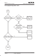
NPM–9 Troubleshooting Instructions PAMS Technical Documentation Charging fault Connect (ACP–7) charger Charger Battery bar doesn‘t work (scroll) No Retest Yes Measure voltage over (TVS) V100. Is it > 3.0 Vdc ? No Check X100, V100, C103, C100, F100, L100 and line Yes Read BTEMP value. (Compare it to ambient temperature) Is it ~ 25 C (0319) ? No Check X101,C109 R202, C240, R203 and line. Yes Remove (fuse) F100 No and measure current. Is it ~350...
NPM–9 Troubleshooting Instructions PAMS Technical Documentation SIM card is out of order (insert SIM card) SIM card Insert SIM card faults No Yes No Set phone LOCAL mode Is it OK ? Check BSI line X101, C241, R203, C109, R202. If OK –> Change UEM Yes Check X386 Measure VSIM voltge from X386 Is it 3V ? No Check VSIM line,X386, C203, C389. If OK –> Change R388. If still wrong VSIM voltage –> Change UEM Yes Check SIM power UP sequency (Page 35 figure 19) Is it OK ? No Check SIM lines.
NPM–9 Troubleshooting Instructions PAMS Technical Documentation Audio fault Audio faults No Is earpiece working? Yes Try change earpiece. Yes Is it working now ? Retest No Set phone in LOCAL mode. Use Phoenix Audio Test. Set EXT IN, HP OUT, LOOP ON. Measure DC offset voltage from Earpiece pads. Is it ~1.38V ? No Check L151, C160, R164 and line. If OK –> Change UEM Yes Measure MICB2 No voltage from XMICP pads (L106) . Is it ~2.2V ? Check L106, C112, R161, C163, R166, C165, R167 and line.
NPM–9 Troubleshooting Instructions PAMS Technical Documentation Earpiece 2 Connect EXT audio signal 1kHz (sine) (¨200mVp–p) in XMICP pads and Ground in XMICN Measure sine signal from earpiece pads. Is it ~880mVp–p ? No Measure sine signal from UEM (R156) Is it ~130mVp–p ? Change UEM. No Yes Check R156, C153, C155, R166, R167, C163, R161 and line.
NPM–9 Troubleshooting Instructions PAMS Technical Documentation Audio faults 2 Is microphone working? Yes No Try change bottom connector X100. Is it working now ? Yes Retest No Set phone in LOCAL mode. Use Phoenix Audio Test. Set HP IN, EXT OUT, LOOP ON. Measure MICB1 No voltage from MICP pads. Is it ~2.1V ? Check L105, C105, C152, C156, R152, C168, C166, C215 and line. If OK –> Change UEM Yes Check C151, R157, C105, C154 and line.
NPM–9 Troubleshooting Instructions PAMS Technical Documentation Audio faults 3 Is BUZZER working? Yes No Measure VBATT voltage from B301. Is it OK? No Check VBATT line Yes Set phone in LOCAL mode. Use Phoenix Audio Test. Set Buzzer volume ON. Measure Buzzer Yes control signal from BUZZER (C307). Is it 1kHz pulses ? Change BUZZER (B301) No Check C306, C307, C308 and line.
NPM–9 Troubleshooting Instructions PAMS Technical Documentation Display fault Display faults Set phone into local mode. Start Display test with Phenix Try change UI module Yes Is it working now ? Are the UI–module led’s turned on ? No Retest No Check X303 Yes Measure signal from X303 pin. 2. Is it 128 Hz ~3.3Vp–p ? Yes Check X303 No Check R306 If OK. Measure VBATT from V300 pin. 4 Is it OK? No Yes Measure PWM LED‘s No control signal from UEM Is it 128 Hz ~3.
NPM–9 Troubleshooting Instructions PAMS Technical Documentation Display faults 2 Are the display led’s turned on ? Yes No Measure signal fromV301 pin. 3. Is it 128 Hz ~3.3Vp–p ? Yes Check LED‘s and line No Check R307 and VBATT line No Measure VBATT from V301 pin. 4 It is OK? Yes Measure PWM LED‘s No control signal from UEM Is it 128 Hz ~3.8Vp–p ? Check control signal line.
NPM–9 Troubleshooting Instructions PAMS Technical Documentation Display faults 3 Try change UI module Yes Is it working now ? Retest No Does the display start ? No Yes Check X300 Measure VDD (2.78V) and VDDI (1.8V). Is it OK? No Check C303 and lines. If OK, Change UEM Yes Measure VOUT voltage. Is it ~8.1V? No Check C302, X300 and lines. Yes Measure XRES, XCS. Is it ~1.8 V? No Check X300 and lines.
NPM–9 Troubleshooting Instructions PAMS Technical Documentation Keypad fault Keypad faults Measure voltage from S300 Is it HIGH ? No Is the power key working ? Yes Check R301, C312, S300 and line. If OK –> Change UEM No Yes Measure voltage Yes from S300 when power key is pressed. Is it HIGH ? No Chech S300.
NPM–9 Troubleshooting Instructions PAMS Technical Documentation Keypad faults 2 Try change UI module. Yes Is it working now ? No Is UI module keys working ? Retest No Check X303 Yes Measure ROW0, ROW1, ROW2, ROW3, No ROW4 lines from X303. Are they ~1.8V ? Check ROW0 – 4 Lines, X303. If OK change Z301. If still fail change UPP Yes Measure SLEEPX No signal from J403 when key is pressed. Is it ~1.8V? Check ROW0 – 4 Lines, X303. If OK change Z301.
NPM–9 Troubleshooting Instructions PAMS Technical Documentation Keypad faults 3 No Is volume UP key working ? Measure ROW0 line from S301. Is it ~1.8 V ? Yes No Check S301, S302, lines. If OK change Z301. If still FAIL change UPP Yes Measure COL1 from S301 when S301 is pressed Is there 50us pulse ? No Check S301 and COL1 line. If OK change Z301. If still FAIL change UPP Yes Change UPP Is volume DOWN key No working ? Yes END Measure ROW0 line from S302. Is it ~1.
NPM–9 Troubleshooting Instructions PAMS Technical Documentation RF Troubleshooting Introduction Measurements should be done using spectrum analyzer with high–frequency high–impedance passive probe (LO–/reference frequencies and RF power levels) and oscilloscope with a 10:1 probe (DC–voltages and low frequency signals). The RF–section is build around one RF–ASIC (HAGAR N600). Before changing HAGAR, please check following things: Supply voltages are OK and serial communication coming from baseband to HAGAR.
NPM–9 Troubleshooting Instructions PAMS Technical Documentation RF Key Components EGSM LNA EGSM TX SAW GSM1800 LNA GSM1800 TX balun Dual RX SAW GSM1800 RX 2nd SAW EGSM RX 2nd SAW Dual coupler Antenna switch Antenna pad Dual PA Issue 1 02/2002 FM IF filter 2 Hagar RFIC 26MHz XO VCO balun 4GHz VCO FM receiver IC FM IF filter 1 FM diskriminator Nokia Corporation Page 25
NPM–9 Troubleshooting Instructions PAMS Technical Documentation PWB Test Points 900 1st SAW out 1800 LNA out 1800 1st SAW out LNA_P LNAB_G 900_RX LNAB_P VR2 900 LNA out VrefRf02 900 antsw tx contr VrefRf01 VR5 RX_I LNA_G VR4 VR6 RX_Q 1800 antsw contr 1800_RX 1800 PA ctrl Antenna pad 900 PA ctrl 900 PA bias 1800 PA bias 900 PA in 900 Mod out 1800 Mod out 1800 PA in Page 26 FMdiscr.
PAMS Technical Documentation NPM–9 Troubleshooting Instructions Transmitter General instructions Connect test jig to computer with DAU9S cable or to FPS–8 Flash Prommer with XCS–4 modular cable. Make sure that you have PKD–1 dongle connected to computers parallel port. Connect DC power supply to module test jig with FLC–2 cable. NOTE: When repairing or tuning transmitter use external DC supply with at least 3A current capability. Set the DC supply voltage to 3.
NPM–9 Troubleshooting Instructions PAMS Technical Documentation Transmitter troubleshooting diagram Page 28 Nokia Corporation Issue 1 02/2002
PAMS Technical Documentation Issue 1 02/2002 Nokia Corporation NPM–9 Troubleshooting Instructions Page 29
NPM–9 Troubleshooting Instructions Page 30 Nokia Corporation PAMS Technical Documentation Issue 1 02/2002
NPM–9 Troubleshooting Instructions PAMS Technical Documentation Transmitter signals TX_I_0, Tx on, Random data, Burst mode TX_Q_0, Tx on, Random data, Burst mode 900/1800 antsw tx contr, Tx on, Burst mode 900/1800 PA bias, Tx on, Burst mode Issue 1 02/2002 900/1800 PA ctrl, Tx on, Burst mode, High power level Nokia Corporation Page 31
NPM–9 Troubleshooting Instructions G S MP O W RE F 4 1 . 0 1 0 d B/ d Bm PAMS Technical Documentation ATT 40 Tu e Se p 2 5 1 3 : 4 8 : 5 9 2 0 0 1 A_ wr i t eB_ b l a n k dB REF OFS 11. 0 dB RB W 100 VBW 100 S WP 2. 0 k Hz k Hz s CE NT E R 897. 400 MH z SPAN 2.
PAMS Technical Documentation NPM–9 Troubleshooting Instructions Receiver General instructions Connect test jig to computer with DAU9S cable or to FPS–8 Flash Prommer with XCS–4 modular cable. Make sure that you have PKD–1 dongle connected to computers parallel port. Connect DC power supply to module test jig with FLC–2 cable. Set the DC supply voltage to 3.9V and set the jumper connector on test jig to ”bypass” position.
NPM–9 Troubleshooting Instructions PAMS Technical Documentation Receiver troubleshooting diagram for GSM900 Apply –90dBm 942.46771MHz signal from generator to antenna connector Yes Oscilloscope at RX_I Signal 700mVpp DC offset 1.35V Frequency 67.
NPM–9 Troubleshooting Instructions PAMS Technical Documentation Receiver troubleshooting diagram for GSM1800 Apply –90dBm 1842.86771MHz signal from generator to antenna connector Yes No Oscilloscope at RX_I Signal 700mVpp DC offset 1.35V Frequency 67.
NPM–9 Troubleshooting Instructions PAMS Technical Documentation LNA gainstep checking GSM900 & GSM1800 900 LNA out – RF–level at antenna port eg. –50 dBm – RX continuous mode (local mode) – difference between AGC –settings ”FEG on” and ”FEG off” roughly 25 dB (using 250 ohm passive RF–probe) 1800 LNA out – RF–level at antenna port eg.
PAMS Technical Documentation NPM–9 Troubleshooting Instructions Synthesizer General instructions Connect test jig to computer with DAU–9S cable or to FPS–8 Flash Prommer with XCS–4 modular cable. Make sure that you have PKD–1 dongle connected to computers parallel port. Connect DC power supply or FPS–8 to module test jig with FLC–2 cable. Set the DC supply voltage to 3.9V and set the jumper connector on test jig to ”bypass” position. Set the phone module to test jig and start Phoenix service sofware.
NPM–9 Troubleshooting Instructions PAMS Technical Documentation Synthesizer troubleshooting diagram Page 38 Nokia Corporation Issue 1 02/2002
NPM–9 Troubleshooting Instructions PAMS Technical Documentation Synthesizer signals 26MHz XO out 13MHz clock 4GHz VCO ctrl 900 RX, channel 124, continuous mode Issue 1 02/2002 4GHz VCO ctrl 1800 TX, channel 512, continuous mode Nokia Corporation Page 39
NPM–9 Troubleshooting Instructions REF – 2 0 . 0 1 0 d B/ MK R 3. 610400 d Bm PAMS Technical Documentation ATT 10 Fr i dB Ma y 1 1 1 3 : 0 3 : 2 6 2 0 0 1 A_ v i e wB_ b l a n k MA R K E R 3 . 6 1 0 4 0 0 GH z – 3 0 . 7 2 d Bm GH z RB W 1 0 k Hz VBW 1 0 k Hz S WP 5 0 ms CE NT E R 3. 6104000 GH z SPAN 2.
PAMS Technical Documentation NPM–9 Troubleshooting Instructions FM Radio troubleshooting FM Radio component layout Components L101, C101 and C102 are not shown in picture. Components are placed in baseband section.
NPM–9 Troubleshooting Instructions PAMS Technical Documentation FM Radio troubleshooting diagram Note 1. RF test signal parameters: – Amplitude, A, –67.0 dBm – Carrier ferquency, fc , 98,000 MHz – Deviation, ∆f, 75 kHz – Modulating frequency fm , 1,000 kHz (RF generator internal) Note 2. Use 10x probe. Compare measured RF signal level to a known good product.
NPM–9 Troubleshooting Instructions PAMS Technical Documentation FM Radio signals Audio out from PWB test point – with FM test signal. G S MP O W RE F – 3 0 . 0 1 0 d B/ CE NT E R 98. 0000 d Bm ATT 0 Fr i dB Audio out from test jig connector – with FM test signal, volume 100%. Au g 3 1 0 7 : 4 0 : 2 1 2 0 0 1 A_ v i e wB_ b l a n k G S MP O W RE F – 3 0 . 0 1 0 d B/ CE NT E R 108. 7000 MH z REF OFS 0.
NPM–9 Troubleshooting Instructions PAMS Technical Documentation This page intentionally left blank.