PAMS Technical Documentation NPM–9 Series Transceivers System Module & UI Issue 1 02/2002 Nokia Corporation
NPM–9 System Module & UI PAMS Technical Documentation CONTENTS Transceiver NPM–9 . . . . . . . . . . . . . . . . . . . . . . . . . . . . . . . . . . . . . Introduction . . . . . . . . . . . . . . . . . . . . . . . . . . . . . . . . . . . . . . . . . . Electrical Modules . . . . . . . . . . . . . . . . . . . . . . . . . . . . . . . . . . Operation Modes . . . . . . . . . . . . . . . . . . . . . . . . . . . . . . . . . . . Interconnection Diagram . . . . . . . . . . . . . . . . . . . . . . . . . . . . . .
PAMS Technical Documentation NPM–9 System Module & UI RF characteristics . . . . . . . . . . . . . . . . . . . . . . . . . . . . . . . . . . Transmitter characteristics . . . . . . . . . . . . . . . . . . . . . . . . Receiver characteristics . . . . . . . . . . . . . . . . . . . . . . . . . . RF Block Diagram . . . . . . . . . . . . . . . . . . . . . . . . . . . . . . . . . . Frequency synthesizers . . . . . . . . . . . . . . . . . . . . . . . . . . . . . Receiver . . . . . . . . . . . . . . . . . . . . .
NPM–9 System Module & UI PAMS Technical Documentation This page intentionally left blank.
PAMS Technical Documentation NPM–9 System Module & UI Transceiver NPM–9 Introduction The NPM–9 is a dual band radio transceiver unit for the E–GSM900 and GSM1800 networks. GSM power class is 4 and GSM1800 power class is 1. It is a true 3 V transceiver, with an internal antenna and vibra. The NPM–9 phone includes integrated FM radio. Radio is used as a normal mono receiver. FM radio is highly integrated. Only few external components are needed. Headset is used as an antenna for radio.
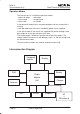
NPM–9 System Module & UI PAMS Technical Documentation Operation Modes The transceiver has six different operation modes: – power off mode – active mode – local mode – idle mode – charge mode – test mode In the power off mode circuits are powered down and only sleep clock is running. In the idle mode only the circuits needed for power up are supplied. In the active mode all the circuits are supplied with power although some parts might be in the idle state part of the time.
NPM–9 System Module & UI PAMS Technical Documentation System Module LA5 Baseband Module The baseband architecture supports a power saving function called ”sleep mode”. This sleep mode shuts off the VCTCXO, which is used as system clock source for both RF and baseband. During the sleep mode the system runs from a 32 kHz crystal. The phone is waken up by a timer running from this 32 kHz clock supply. The sleep time is determined by network parameters.
NPM–9 System Module & UI PAMS Technical Documentation Technical Summary Baseband is running from power rails 2.8V analog voltage and 1.8V I/O voltage. UPP core voltage Vcore can be lowered down to 1.0V, 1.3V and 1.5V. UEM includes 6 linear LDO (low drop–out) regulators for baseband and 7 regulators for RF. It also includes 4 current sources for biasing purposes and internal usage. UEM also includes SIM interface which has supports both 1.8V and 3V SIM cards.
NPM–9 System Module & UI PAMS Technical Documentation DC Characteristics Regulators and Supply Voltage Ranges Battery Voltage Range Signal VBAT Min 3.1V Nom 3.6V Max Note 4.2V (charging 3.1V SW cut off high limit voltage) BB Regulators Signal Min Nom Max Note VANA 2.70V 2.78V 2.86V Imax = 80mA VFLASH1 2.70V 2.78V 2.86V Imax = 70mA ISleep = 1.5mA VFLASH2 2.70V 2.78V 2.86V Imax = 40mA VSIM 1.745V 1.8V 1.855V Imax = 25mA 2.91V 3.0V 3.09V ISleep = 0.5mA 1.72V 1.8V 1.
NPM–9 System Module & UI PAMS Technical Documentation External and Internal Signals and Connections This section describes the external and internal electrical connection and interface levels on the baseband. The electrical interface specifications are collected into tables that covers a connector or a defined interface. Internal Signals and Connections FM Radio Interface BB Signal VFLASH2 GenIO(3) FM Radio Signal Min Nom Max 2.7V 2.78V 2.86V max. Icc1 19mA Vcc2 2.7V 2.78V 2.86V max.
NPM–9 System Module & UI PAMS Technical Documentation BB Signal GenIO(12) FM Radio Signal FMCtrlDa Min 1.4V 0 Nom 1.8V Max Condition Note 1.88V 0.4V High Low Bidirectional 14us tda shift register available after ”search ready” 10 µs tshift data available after FMCtrlClk rising edge (read operation) 1.5 µs thold FMCtrlDa stabile after FMCtrlClk rising edge (write operation) High Low from FM module to UPP (FMCtrlClk = ’1’) GenIO(27) FMTuneX 1.4V 0 1.8V 1.88V 0.
NPM–9 System Module & UI PAMS Technical Documentation AC and DC Characteristics of RF–BB voltage supplies Signal name VBAT From Battery To PA & UEM Parameter Voltage Min Typ Max 2.95 3.6 4.2 Current UEM Voltage VCP 4.6 Current 0.8 2 uA 4.75 4.9 V 2 10 mA 240 nVrms/ sqrt(Hz) 2.78 2.86 V 65 100 mA 120 nVrms/ sqrt(Hz) 2.78 2.86 V 1 20 mA 240 nVrms/ sqrt(Hz) Noise density VR2 UEM VRF_TX Voltage 2.
NPM–9 System Module & UI PAMS Technical Documentation Signal name VR7 From UEM To Parameter Voltage UHF VCO VrefRF01 UEM VREF_RX Min Typ Max 2.70 2.78 2.86 V Supply for UHF VCO 30 mA Noise density 100Hz
NPM–9 System Module & UI Signal name PAMS Technical Documentation From To Parameter Min RFBusEna1X UPP RF–IC Typ Max ”1” 1.38 1.88 V ”0” 0 0.4 V 50 uA 220 kohm 20 pF Current Load resistance 10 Load capacitance RFBusData RFBusClk RESET (GENIO6) UPP UPP UPP RF–IC RF–IC RF–IC Fun ction Unit ”1” 1.38 1.88 V ”0” 0 0.4 V Load resistance 10 220 kohm Load capacitance 20 pF Data frequency 10 MHz ”1” 1.38 1.88 V ”0” 0 0.
NPM–9 System Module & UI PAMS Technical Documentation Signal name TXIP / TXIN From UEM To RF–IC Parameter Min Differential voltage swing (static) 2.23 DC level 1.17 Typ 1.20 Source Impedance TXQP / TXQN UEM RF–IC AFC UEM VCTCXO Voltage Min Max UEM 0.0 2.4 Resolution 11 Load resistance and capacitance 1 Voltage Min Max RF V 200 ohm UEM UEM 100 kohm nF 0.2 ms 0.1 V 200 ohm 800 –65 +65 1,57 Voltage at +25oC 1,7 +60oC Programmable voltage swing.
NPM–9 System Module & UI Pin PAMS Technical Documentation Signal Min Nom Max Condition Note 4 ROW(3) 0.7xVIO 0 VIO 0.3xVIO High Low Keyboard matrix row 3 5 COL(2) 0.7xVIO 0 VIO 0.3xVIO High Low Keyboard matrix column 2 6 ROW(2) 0.7xVIO 0 VIO 0.3xVIO High Low Keyboard matrix row 2 7 COL(1) 0.7xVIO 0 VIO 0.3xVIO High Low Keyboard matrix column 1 8 ROW(0) 0.7xVIO 0 VIO 0.3xVIO High Low Keyboard matrix row 0 9 KLIGHT VBAT 0.
NPM–9 System Module & UI PAMS Technical Documentation Pin 5 6 Signal SCLK Min Nom Max 0.8*VIO 0 VDDI (VIO) Condition VIO 0.22*VIO 4.0MHz Note Logic ’1’ Logic ’0’ Max frequency Serial clock input 250ns tscyc Clock cycle 110ns tshw Clock high 110ns tslw Clock low 1.72V 1.8V 1.88V Logic voltage supply Connected to VIO 7 VDD (VFLASH1) 2.72V 2.78V 2.
NPM–9 System Module & UI PAMS Technical Documentation SIM connector Pin Name Parameter Min Typ Max Unit Notes 1 VSIM 1.8V SIM Card 1.6 1.8 1.9 V Supply voltage 3V SIM Card 2.8 3.0 3.2 V SIM reset (output) MHz SIM clock 2 SIMRST 1.8V SIM Card 3V SIM Card 3 0.9xVSIM VSIM 0 0.15xVSIM 0.9xVSIM VSIM 0 0.15xVSIM SIMCLK Frequency 3.25 Trise/Tfall 4 DATA 5 NC 6 GND Page 18 1.8V Voh 0.9xVSIM 1.8V Vol 0 3 Voh 0.9xVSIM 3 Vol 0 50 ns VSIM V VSIM 1.8V Voh 0.
PAMS Technical Documentation NPM–9 System Module & UI Functional Description Modes of Operation LA5 baseband engine has six different operating modes: – No supply – Backup – Acting Dead – Active – Sleep – Charging No supply In NO_SUPPLY mode the phone has no supply voltage. This mode is due to disconnection of main battery and backup battery or low battery voltage level in both of the batteries. Phone is exiting from NO_SUPPLY mode when sufficient battery voltage level is detected.
NPM–9 System Module & UI PAMS Technical Documentation 2.78V or 3.3V. VR4 –VR7 can be enabled or disabled or forced into low quiescent current mode. VR3 is always enabled in active mode. Sleep mode Sleep mode is entered when both MCU and DSP are in stand–by mode. Sleep is controlled by both processors. When SLEEPX low signal is detected UEM enters SLEEP mode. VCORE, VIO and VFLASH1 regulators are put into low quiescent current mode. All RF regulators are disabled in SLEEP.
NPM–9 System Module & UI PAMS Technical Documentation Battery Li–ion battery pack BLB–2 is used in NPM–9. Nominal discharge cut–off voltage 3.1V Nominal battery voltage 3.6V Nominal charging voltage 4.
NPM–9 System Module & UI PAMS Technical Documentation the DSP. During this reset phase the UEM forces the VCTCXO regulator on regardless of the status of the sleep control input signal to the UEM. The FLSRSTx from the ASIC is used to reset the flash during power up and to put the flash in power down during sleep. All baseband regulators are switched on at the UEM power on except SIM and VFLASH2 regulators which are controlled by the MCU.
NPM–9 System Module & UI PAMS Technical Documentation FM Radio FM radio circuitry is implemented using highly integrated radio IC, TEA5757. Only few external components like filters, discriminator and capacitors are needed. TEA5757 is an integrated AM/FM stereo radio circuit including digital tuning and control functions. NPM–9 radio is implemented as superheterodyne FM mono receiver.
NPM–9 System Module & UI PAMS Technical Documentation IR Module The IR interface, when using 2.7V transceiver, is designed into the UEM. The IR link supports speeds from 9600 bit/s to 1.152 MBit/s up to distance of 1m. Transmission over the IR if half–duplex. The lenght of the transmitted IR pulse depends on the speed of the transmission. When 230.4 kbit/s or less is used as a transmission speed, pulse length is maximum 1.63us. If transmission speed is set to 1.
NPM–9 System Module & UI PAMS Technical Documentation The data communication between the card and the phone is asynchronous half duplex. The clock supplied to the card is in GSM system 1.083 MHz or 3.25 MHz. The data baud rate is SIM card clock frequency divided by 372 (by default), 64, 32 or 16. The protocol type, that is supported, is T=0 (asynchronous half duplex character transmission as defined in ISO 7816–3).
NPM–9 System Module & UI PAMS Technical Documentation UEM 22pF 100nF MIC1B MIC1N 33nF 2k2 33nF 2k2 600Ω@100MHz MIC1P 27pF 22pF UPP UPP (Universal Phone Processor) is the digital ASIC of the baseband. UPP includes 8MBit internal RAM, ARM7 Thump 16/32–bit RISC MCU core, LEAD3 16–bit DSP core, ROM for MCU boot code and all digital control logic. Main functions of the custom logic are: 1. Interface between system logic and MCU/DSP (BodyIf) 2.
PAMS Technical Documentation NPM–9 System Module & UI MCU code is stored into external flash memory. Size of the flash is 64Mbit (4096 x 16bit) The NPM–9 baseband supports a burst mode flash with multiplexed address/data bus. Access to the flash memory is performed as 16–bit access. The flash has Read While Write capabilities which makes the emulation of EEPROM within the flash easy.
NPM–9 System Module & UI PAMS Technical Documentation RF Module This RF module takes care of all RF functions of the engine. RF circuitry is located on one side (B–side) of the PWB. EMC leakage is prevented by using a metal B–shield, which screens the whole RF side (included FM radio) of the engine. The conductive (silicon or metal) gasket is used between the PWB and the shield. The metal B–shield is separated to three blocks. The first one include the FM radio.
NPM–9 System Module & UI PAMS Technical Documentation DC characteristics Regulators Transceiver has a multifunction power management IC on baseband section, which contains among other functions; 7 pcs of 2.78 V regulators and 4.8V up–switcher for charge pump. All regulators can be controlled individually with 2.78 V logic directly or through control register. In GSM direct controls are used to get fast switching, because regulators are used to enable RF–functions.
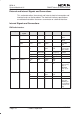
NPM–9 System Module & UI PAMS Technical Documentation Power Distribution Diagram SOURCE VR1 VR2 VR3 LOAD 4.75 V +/– 3.2 % 10 mA 2.78 V +/– 3 % 100 mA 2.78 V +/– 3 % 20 mA Charge pump in HAGAR TX IQ modulator, power control opamp in Hagar VCTCXO VCTCXO buffer in Hagar VR4 2.78 V +/– 3 % 50 mA E–GSM & DCS LNA RX mixer in Hagar DTOS in Hagar VR5 2.78 V +/– 3 % 50 mA PLL in Hagar Dividers in Hagar LO buffers in Hagar UEM Prescaler in Hagar Power detector VR6 2.78 V +/– 3 % 50 mA VR7 2.
NPM–9 System Module & UI PAMS Technical Documentation RF characteristics Item Values (E–GSM / GSM1800) Receive frequency range 925 ... 960 MHz / 1805...1880 MHz Transmit frequency range 880 ... 915 MHz / 1710...
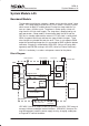
HAGAR I Q LNA SAW f/2 VrefRF01 f EGSM PCN VrefRF02 CTRL NPM–9 System Module & UI LNA RF Block Diagram Page 32 Dual SAW SAW Nokia Corporation SERIAL CTRL BUS f/2 ANT SW f SHF VCO PLL f f/2 f Coupler 13 MHz to ASIC f/2 f AFC 26 MHz VCXO TXC TXP Issue 1 02/2002 PCN Dual PA EGSM SAW TXIP TXIN TXQP TXQN RF_temp PAMS Technical Documentation f/2
NPM–9 System Module & UI PAMS Technical Documentation Frequency synthesizers VCO frequency is locked with PLL into stable frequency source, which is a VCTCXO–module ( voltage controlled temperature compensated crystal oscillator ). VCTCXO is running at 26 MHz. Temperature drifting is controlled with AFC ( automatic frequency control ) voltage. VCTCXO is locked into frequency of the base station. AFC is generated by baseband with a 11 bit conventional DAC.
NPM–9 System Module & UI PAMS Technical Documentation frequency. LO signal is divided by two or four in HAGAR (depending on system mode). Receiver Receiver is a direct conversion, dual band linear receiver. Received RF– signal from the antenna is fed via RF–antenna switch module to 1st RX bandpass RF–SAW filters and MMIC LNAs (low noise amplifier). RF–antenna switch module contains upperband and lowerband operation. The LNA amplified signal is fed to 2nd RX bandpass RF–SAW filters.
PAMS Technical Documentation NPM–9 System Module & UI DC compensation is made during DCN1 and DCN2 operations (controlled via serial bus). DCN1 is carried out by charging the large external capacitors in AGC stages to a voltage which cause a zero dc–offset. DCN2 set the signal offset to constant value (VrefRF_02 1.35 V). The VrefRF_02 signal is used as a zero level to RX ADCs. Single ended filtered I/Q–signal is then fed to ADCs in BB. Input level for ADC is 1.45 Vpp max.
NPM–9 System Module & UI PAMS Technical Documentation RC–filter in AFC control line to reduce the noise from the converter. Settling time requirement for the RC–network comes from signalling, how often PSW ( pure sine wave ) slots occur. They are repeated after 10 frames. AFC tracks base station frequency continuously, so transceiver has a stable frequency, because changes in VCTCXO–output don’t occur so fast ( temperature ). Settling time requirement comes also from the start up–time allowed.
NPM–9 System Module & UI PAMS Technical Documentation UI Board LU9 NPM–9 consists of separate UI board, named as LU9, which includes contacts for the keypad domes and LEDs for keypad illumination. UI board is connected to main PWB through 16 pole board–to–board connector with springs. Signals of the connector are described in section External and Internal Signals and Connections. 5x4 matrix keyboard is used in NPM–9. Key pressing is detected by scanning procedure.
NPM–9 System Module & UI PAMS Technical Documentation LEDs are controlled by the UEM PWM outputs. Both LEDs are controlled by KLight output of the UEM. Current flow through the LEDS is set by biasing the transistor and limiting the current by resistors. Current is set separately to keyboard and LCD leds. Internal Speaker The internal earpiece is a dynamic earpiece with an impedance of 32 ohms.