
Integration Manual


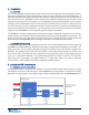


Table Of Contents
- Contents
- List of Figures
- 1. Introduction
- 2. Application PCB Consideration
- 3. Application Hardware Implementation
- 4. RF Guidelines
- 5. Regulatory Compliance Consideration
- 6. Production Testing Consideration
- 7. Regulatory and Compliance Notice
- 8. References
- 9.
- 10. Revision History
- 11. Document Details

NM180100 Hardware Integration Manual-0.9
4
1. Introduction
1.1. Overview
The successful development of a wireless product requires a system level approach where all disciplines must be
taken into consideration during the planning stage. There are many approaches to product development. A
typical development workflow begins with the industrial design including overall cosmetic of the product and the
user interaction elements. Afterwards, an antenna floor plan is developed to identify the general locations of all
the antennas that would exist in the product. This is followed by the general mechanical stack-up such as where
the battery and the PCB would be located. Finally, the major electrical component placement is determined such
as wireless transceiver or power management IC locations. A detailed exposition of wireless product development
is beyond the scope of the present discussion. This manual focuses on the necessary requirements for a successful
integration of the NM180100 and the corresponding antenna design considerations.
The NM180100 is a highly integrated device with significant signal conditioning integrated onto the module.
Careful PCB layout is important to obtain the optimal performance while meeting regulatory requirements. The
goal of this document is to enable designer engineers without RF or analog background to achieve the optimal
performance from the NM180100 while minimizing the fabrication cost and the board layout effort.
1.2. NM180100 Description
The NM180100 integrates an Ambiq Apollo3 microcontroller and a Semtech SX1262 LoRa transceiver supporting
the 868MHz and 915MHz ISM bands. Bluetooth 5 Low Energy is integrated with the Apollo3 microcontroller. The
Apollo 3 possesses a secure interface (ISO 7816) including secure boot and secure OTA firmware upgrade over
Bluetooth. The operating system, radio drivers and wireless communication protocol stacks are provided in the
form of source code. This enables the system integrator to fully leverage the module’s existing regulatory grants
(such as IC or FCC) where applicable. Full programmability allows the module to function as a host while
maintaining all RF, mixed-signals, and digital functions in a single device without the need for additional
microcontrollers. A block diagram of the major components is shown in Figure 1.
2. Application PCB Consideration
2.1. PCB Stackup Recommendations
The NM180100 module is designed to be routable in a conventional PCB stackup without making use of HDI
technologies such as micro or blind/buried vias. While NM180100 can be integrated into a 2-layer stack in simple
applications, a 4-layer stackup is recommended. Figure 3 shows the PCB stackup used in the NM180100EVB where
Figure 1 NM module block diagram