
User Manual
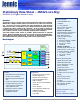
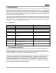
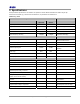
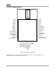
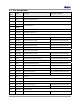
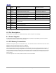
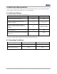
Table Of Contents

Jennic
2. Specifications
Most specification parameters for the modules are specified in JN-DS-JN5121 Datasheet for JN5121 single chip
wireless microcontroller
, [2]. Where there are differences, the parameters are defined here.
VDD=3.0V @ +25ºC
Typ. DC Characteristics Notes
JN5121-xxx-
M00/01/03
JN5121-xxx-
M02/04
Deep sleep <11uA <11uA
Sleep <14uA <14uA With active sleep timer
Radio transmit 44mA 115mA CPU in doze, radio transmitting
Radio receive 49mA 60mA CPU in doze, radio receiving
Centre frequency accuracy +/-25ppm +/-25ppm
Additional +/-15ppm allowance for
temperature and aging
Typ. RF Characteristics Notes
Receive sensitivity -90dBm -93dBm
Nominal for 1% PER, as per
802.15.4 section 6.5.3.3
Max. Transmit power 0dBm 16dBm Nominal
Transmit power at 3.6V 18.5dBm With Vcc=3.6V
Maximum input signal -10dBm -15dBm
For 1% PER, measured as
sensitivity
RSSI range
-95 to -10
dBm
-115 to -20
dBm
RF Port impedance - SMA connector 50 ohm 50 ohm 2.4 - 2.5GHz
VSWR (max) 2:1 2:1 2.4 - 2.5GHz
Peripherals Notes
Master SPI port with five select outputs 250kHz - 16MHz
Slave SPI port 250kHz - 16MHz
Two UARTs 16550 compatible
Two-wire serial I/F (compatible with SMbus & I
2
C) Up to 400kHz
Two programmable Timer/Counters with
capture/compare facility, Tick timer
16MHz clock
Two programmable Sleep Timers 32kHz clock
Twenty-one digital IO lines (multiplexed with
UARTs, timers and SPI selects)
Four-channel, 12-bit, Analogue-to-Digital
converter
Up to 100ks/s
Two 11-bit Digital-to-Analogue converters Up to 100ks/s
Programmable analogue comparator Ultra low power mode for sleep
Internal temperature sensor and battery monitor
2 Preliminary - JN-DS-JN5121-xxx-Myy v1.21 © Jennic 2006