
User Manual
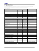
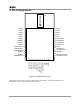
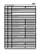
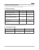
Table Of Contents

Jennic
Module
Pin
Signal Function Alternative Function
31 SIF_D Serial Interface data / Intelligent peripheral data
t
General Purpose Digital I/O DIO15
32 DIO 16 Intelligent peripheral device select General Purpose Digital I/O
33 CTS1 UART1 Clear To Send (input) General Purpose Digital I/O DIO17
34 RTS1 UART1 Request To Send (output) General Purpose Digital I/O DIO18
35 TXD1 UART1 Transmit Data (output) General Purpose Digital I/O DIO19
36 RXD1 UART1 Receive Data (input) General Purpose Digital I/O DIO20
37 DNC
38 DNC
Do Not Connect
39 ADC1 Analogue to Digital input
40 ADC2 Analogue to Digital input
41 ADC3 Analogue to Digital input
*: These two pins are not connected for High power modules
4.2. Pin Descriptions
All pins behave as described in the JN5121 datasheet [2], with the exception of the following:
4.3. Power Supplies
A single power supply pin, VDD is provided. Separate analogue (VSSA) and digital (GND) grounds are provided.
These should be connected together at the module pins.
4.4. SPI Memory Connections
SPISWP is a write protect pin for the serial flash memory. This should be held low to inhibit writes to the flash device.
SPISSZ is connected to SPI Slave Select 0 on the JN5121.
SPISSM is connected to the Slave Select pin on the memory.
This configuration allows the flash memory device to be programmed using an external programmer if required. The
JN5121 should be held in reset by taking RESETN low. The memory can then be programmed over the UART by
using the programming mode described in
JN-UG-3007 Flash Loader User Guide [5]. Alternatively, the memory can
be programmed by connecting a SPI programmer to SPISSM, SPICLK, and SPIMISO and directly loading the code
into the memory.
For normal operation of the module, SPISSZ should be connected to SPISSM.
6 Preliminary - JN-DS-JN5121-xxx-Myy v1.21 © Jennic 2006