
User Manual
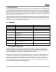
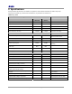
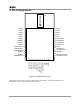
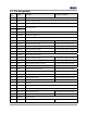
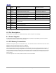
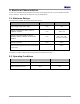
Table Of Contents

Jennic
5. Electrical Characteristics
In most cases, the Electrical Characteristics are the same for both module and chip. They are described in detail in
the chip datasheet. Where there are differences, they are detailed below.
5.1. Maximum Ratings
Exceeding these conditions will result in damage to the device.
Parameter Min Max
Device supply voltage VDD1, VDD2 -0.3V 3.6V
Voltage on analogue pins ADC1-4, DAC1-2,
COMP2M, COMP2P
-0.3V VDD + 0.3V
Voltage on 5V tolerant digital pins SPICLK,
SPIMOSI, SPIMISO, SPISEL0, GPIO0-GPIO20,
RESETN
-0.3V
VDD + 2V or 5.5V,
whichever is the lesser
Storage temperature -40ºC 150ºC
Solder reflow temperature (According to IPC/JEDEC
J-STD-020C)
260 °C
This device is sensitive to ESD and should only be handled using ESD precautions.
5.2. Operating Conditions
Supply Min Max
VDD 2.7V 3.6V
Ambient temperature range -20ºC 70ºC
© Jennic 2006 Preliminary - JN-DS-JN5121-xxx-Myy v1.22 7