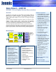
Data Sheet – JN5139 IEEE802.15.4 and ZigBee Wireless Microcontrollers Features: Transceiver Overview The JN5139 is a low power, low cost wireless microcontroller suitable for IEEE802.15.4 and ZigBee applications. The device integrates a 32-bit RISC processor, with a fully compliant 2.4GHz IEEE802.15.4 transceiver, 192kB of ROM, 96kB of RAM, and a rich mixture of analogue and digital peripherals.
Jennic 1 Introduction 6 1.1 1.2 1.3 1.4 1.5 6 6 6 7 8 Wireless Microcontroller Wireless Transceiver RISC CPU and Memory Peripherals Block Diagram 2 Pin Configurations 2.1 2.2 2.2.1 2.2.2 2.2.3 2.2.4 2.2.5 2.2.6 9 Pin Assignment Pin Descriptions Power Supplies Reset 16MHz System Clock Radio Analogue Peripherals Digital Input/Output 10 11 11 11 11 11 11 12 3 CPU 13 4 Memory Organisation 14 4.1 4.2 4.3 4.4 4.4.1 4.5 4.
Jennic 8.3.2 8.3.3 8.3.4 8.3.5 8.4 Reception Auto Acknowledge Beacon Generation Security Security Coprocessor 27 27 27 27 27 9 Digital Input/Output 29 10 Serial Peripheral Interface 30 11 Intelligent Peripheral Interface 33 11.1 11.2 11.3 33 34 34 Data Transfer Format JN5139 Initiated Data Transfer Remote Processor Initiated Data Transfer 12 Timers 35 12.1 Peripheral Timer / Counters 12.1.1 Pulse Width Modulation Mode 12.1.2 Capture Mode 12.1.3 Counter / Timer Mode 12.1.4 Delta-Sigma Mode 12.
Jennic 16.3.3 Comparator Event 16.4 Deep Sleep Mode 49 49 17 Electrical Characteristics 50 17.1 Maximum ratings 17.2 DC Electrical Characteristics 17.2.1 Operating Conditions 17.2.2 DC Current Consumption 17.2.3 I/O Characteristics 17.3 AC Characteristics 17.3.1 Reset 17.3.2 SPI Timing 17.3.3 Two-wire serial interface 17.3.4 Power Down and Wake-Up timings 17.3.5 32kHz Oscillator 17.3.6 16MHz Crystal Oscillator 17.3.7 Bandgap Reference 17.3.8 Analogue to Digital Converters 17.3.
Jennic B.3.12 B.3.13 B.3.14 B.3.15 B.3.16 B.3.17 B.3.18 Bespoke Solutions - PCB Layout Suggestions Using a Balun Decoupling Capacitors Internal Regulator Smoothing Capacitors VREF IBIAS EMC 80 81 81 82 82 82 82 Appendix C 83 Related Documents RoHS Compliance Status Information Disclaimers Version Control Contact Details 83 83 83 84 84 85 © Jennic 2008 JN-DS-JN5139 v1.
Jennic 1 Introduction The JN5139 is an IEEE802.15.4 wireless microcontroller that provides a fully integrated solution for applications using the IEEE802.15.4 standard in the 2.4 - 2.5GHz ISM frequency band [1], including ZigBee. It includes all of the functionality required to meet the IEEE802.15.4 specification and has additional processor capability to run a wide range of applications including but not limited to Remote Control, Home and Building Automation, Toys and Gaming.
Jennic 1.
Jennic 1.5 Block Diagram Tick Timer 32-bit RISC CPU Programmable Interrupt Controller SPICLK SPIMOSI SPIMISO SPISEL0 SPI DIO0/SPISEL1 DIO1/SPISEL2 DIO2/SPISEL3/RFRX DIO3/SPISEL4/RFTX From Peripherals RAM 96kB ROM 192kB UART0 DIO4/CTS0 DIO5/RTS0 DIO6/TXD0 DIO7/RXD0 UART1 DIO17/CTS1/IP_SEL DIO18/RTS1/IP_INT DIO19/TXD1 DIO20/RXD1 OTP eFuse 48-byte M U X VB_xx VDD1 Voltage Regulators VDD2 RESETN 1.
Jennic DIO15/SIF_D/IP_DO DIO14/SIF_CLK/IP_CLK DIO13/TIM1OUT DIO12/TIM1CAP DIO11/TIM1CK_GT DIO10/TIM0OUT DIO9/TIM0CAP/CLK32K VDD2 DIO8/TIM0CK_GT DIO7/RXD0 DIO6/TXD0 DIO5/RTS0 DIO4/CTS0 DIO3/SPISEL4/RFTX 56 55 54 53 52 51 50 49 48 47 46 45 44 43 2 Pin Configurations DIO16/IP_DI 1 42 DIO17/CTS1/IP_SEL 2 41 DIO1/SPISEL2 VB_DIG2 3 40 VB_MEM DIO18/RTS1/IP_INT 4 39 VSS1 DIO19/TXD1 5 38 DIO0/SPISEL1 DIO20/RXD1 6 37 SPISEL0 VSS2 7 36 SPIMOSI RESETN 8 35 VB_
Jennic 2.
Jennic 2.2 Pin Descriptions 2.2.1 Power Supplies The device is powered from the VDD1 and VDD2 pins, each being decoupled with a 100nF ceramic capacitor. VDD1 is the power supply to the analogue circuitry; it should be decoupled to analogue ground. VDD2 is the power supply for the digital circuitry; it should be decoupled to digital ground. A 10uF tantalum capacitor is required at the common ground star point of analogue and digital supplies. Decoupling pins for the internal 1.
Jennic VDD1 Analogue I/O Pin Analogue Peripheral VSSA Figure 3 Analogue I/O Cell 2.2.6 Digital Input/Output Digital I/O pins on the JN5139 can have signals applied up to 2V higher than VDD2 (with the exception of pins DIO9 and DIO10 that are 3V tolerant) and are therefore TTL-compatible with VDD2 > 3V. For other DC properties of these pins see section 17.2.3 I/O Characteristics.
Jennic 3 CPU The CPU of the JN5139 is a 32-bit load and store RISC processor.
Jennic 4 Memory Organisation This section describes the different memories found within the JN5139. The device contains ROM, RAM, OTP eFuse memory, the wireless transceiver and peripherals all within the same linear address space.
Jennic 4.1 ROM The ROM is 192K bytes in size, organized as 48k x 32-bit words and can be accessed by the CPU in a single clock cycle. The ROM contents include bootloader to allow external Flash memory contents to be bootloaded into RAM at runtime, a default interrupt vector table, an interrupt manager, IEEE802.15.4 MAC and assorted APIs for interfacing to the MAC and on-chip hardware peripherals.
Jennic 4.3 OTP eFuse Memory The JN5139 contains 48-bytes of eFuse memory; this is one time programmable memory that is organised as 12 x 32-bit words, 4 words are reserved by Jennic and 4 words are reserved for future use. The remaining 4 words are fully user programmable, designed to allow for the storage of a 128-bit encryption key for secure external memory encryption (see section 4.4.
Jennic With encryption enabled, the speed of bootloading code from external Flash memory is halved. 4.5 Peripherals All peripherals have their registers mapped into the memory space. Access to these registers requires 3 clock cycles. Applications have access to the peripherals through the software libraries that present a high-level view of the peripheral’s functions through a series of dedicated software routines.
Jennic 5 System Clocks Two separate oscillators are used to provide system clocks: a crystal-controlled 16MHz oscillator, using an external crystal and an internal, RC-based 32kHz oscillator. 5.1 16MHz Oscillator The JN5139 contains the necessary on-chip components to build a 16 MHz reference oscillator with the addition of an external crystal resonator and two tuning capacitors. The schematic of these components are shown in Figure 9.
Jennic 6 Reset A system reset initialises the device to a predefined state and forces the CPU to start program execution from the reset vector. The reset process that the JN5139 goes through is as follows. When power is applied, the 32kHz oscillator starts up and stabilises, which takes approximately 100µsec. At this point, the 16MHz crystal oscillator is enabled and power is applied to the processor and digital logic.
Jennic the operation of the internal power-on reset circuit. If complete discharge is difficult to achieve then it is recommended that the external reset circuit, as shown in Figure 11, be used. VDD JN5139 R1 10k RESETN C1 100nF Figure 11: External Reset Generation The external resistor and capacitor provide a simple reset operation when connected to the RESETN pin. 6.2 External Reset An external reset is generated by a low level on the RESETN pin.
Jennic 7 Interrupt System The interrupt system on the JN5139 is a hardware-vectored interrupt system. The JN5139 provides several interrupt sources, some associated with CPU operations (CPU exceptions) and others which are used by hardware in the device. When an interrupt occurs the CPU stops executing the current program and loads its program counter with a fixed hardware address specific to that interrupt.
Jennic 7.3 Hardware Interrupts Hardware interrupts generated from the transceiver, analogue or digital peripherals and DIO pins are individually masked using the Programmable Interrupt Controller (PIC). Management of interrupts is provided in the peripherals library. Further details of interrupts are provided for the functions in their respective sections in this datasheet. Interrupts are used to wake the JN5139 from sleep.
Jennic 8 Wireless Transceiver The wireless transceiver comprises a 2.45GHz radio, an O-QPSK modem, a baseband processor, a security coprocessor and PHY controller. These blocks, with protocol software provided as a library, implement an IEEE802.15.4 standards-based wireless transceiver that transmits and receives data over the air in the unlicensed 2.4GHz band. 8.
Jennic 8.1.1 Radio External components The VCO loop filter requires three external components and the IBIAS pin requires one external component as shown in Figure 15. These components should be placed close to the JN5139 pins and analogue ground. VCOTUNE 15 4k7 1% 19 IBIAS VB_VCO 3n3F 100nF 330pF 43k 1% VSSA VSSA Figure 15: VCO Loop Filter and IBIAS The radio is powered from a number of internal 1.
Jennic ADO (DIO[12]) TX Active RX Active 1st TX-RX Cycle 2nd TX-RX Cycle (1st Retry) Figure 17 Antenna Diversity ADO Signal for TX with Acknowledgement 8.2 Modem The Modem performs all the necessary modulation and spreading functions required for digital transmission and reception of data at 250kbps in the 2450MHz radio frequency band in compliance with the IEEE802.15.4 standard.
Jennic Symbol detection and synchronization is performed using direct sequence correlation techniques in conjunction with searches for the Preamble and Start-of-Frame Delimiter (SFD) fields contained in the transmitted IEEE 802.15.4 Synchronization Header (SHR). Features are provided to support network channel selection algorithms include Energy Detection (ED), Link Quality Indication (LQI) and fully programmable Clear Channel Assessment (CCA).
Jennic algorithms required by IEEE802.15.4 such as CSMA/CA including retries and random backoffs without processor intervention. When the transmission begins, the header of the frame is constructed from the parameters programmed by the software and sent with the frame data through the serialiser to the Modem. At the same time, the radio is prepared for transmission.
Jennic Arbiter Processor Interface In-line Interface AES Block Encrpytion Controller AES Encoder Key Generation Some protocols (for example ZigBee) require that security operations can be performed on buffered data rather than in-line. A hardware implementation of the encryption engine significantly speeds up the processing of the contents of these buffers. The Security Coprocessor can be accessed through software to allow the contents of memory buffers to be transformed.
Jennic 9 Digital Input/Output There are 21 Digital I/O (DIO) pins, which can be configured as either an input or an output, and each has a selectable internal pull-up resistor. Most DIO pins are multiplexed with alternate peripheral features of the device. Once a peripheral is enabled it takes precedence over the device pins. Refer to the individual module sections for a full description of the alternate peripherals functions.
Jennic 10 Serial Peripheral Interface The Serial Peripheral Interface (SPI) allows high-speed synchronous data transfer between the JN5139 and peripheral devices. The JN5139 operates as a master on the SPI bus and all other devices connected to the SPI are expected to be slave devices under the control of the JN5139 CPU.
Jennic SS SO C SS User Defined SI C SO SO C SI SS SS 43 42 C SO User Defined Slave 4 SPISEL1 SPISEL2 SPISEL3 SPISEL4 38 SI 37 SPISEL0 User Defined 41 SS User Defined SO C SI Flash Memory Slave 3 Slave 2 SI Slave 1 Slave 0 36 JN5139 33 SPIMOSI SPICLK 34 SPIMISO Figure 23: Typical JN5139 SPI Peripheral Connection The data transfer rate on the SPI bus is determined by the SPICLK signal.
Jennic A transaction commences with the SPI bus being set to the correct configuration, and then the slave device is selected. Upon commencement of transmission (8, 16 or 32 bits) data is placed in the FIFO data buffer and clocked out, at the same time generating the corresponding SPICLK transitions. Since the transfer is full-duplex, the same number of data bits is being received from the slave as it transmits. The data that is received during this transmission can be read 8, 16 or 32 bits.
Jennic 11 Intelligent Peripheral Interface The Intelligent Peripheral (IP) Interface is provided for systems that are more complex, where there is a processor that requires a wireless peripheral. As an example, the JN5139 may provide a complete IEEE802.15.4, ZigBee or other wireless network to a phone, computer, PDA, set-top box or games console. No resources are required from the main processor compared to a transceiver as the complete wireless protocol may be run on the internal JN5139 CPU.
Jennic has no data to transfer, then the data length should be set to zero. The transaction can be terminated by the master after the status byte has been sent if it is not possible to send data in either direction. This may be because neither party has data to send or because the receiver does not have a buffer available. If the data length is non-zero, the data in the JN5139 transmit memory buffer is sent, beginning at the start of the buffer.
Jennic 12 Timers 12.1 Peripheral Timer / Counters Two general-purpose timer / counter units are available that can be independently configured to operate in one of five modes. The timers have the following features: prescale • 16-bit prescaler, divides system clock by 2 • Clocked from internal system clock • 16-bit counter, 16-bit Rise and Fall (period) registers • Timer: can generate interrupts off Rise and Fall counts.
Jennic The counter is optionally gated by a signal on the clock / gate input (TIMxCK_GT). If the gate function is selected the counter is frozen when the clock/gate input is high. An interrupt can be generated when the counter is equal to the value in either of the High or Low registers. The internal Output Enable (OE) signal enables or disables the timer output.
Jennic 12.1.3 Counter / Timer Mode The counter/timer can be used to generate timing or count interrupts for software to use. As a timer the clock source is from the system clock, prescaled if required. The timer period is programmed into the Fall register and the Fall register match interrupt enabled. The timer is started as either a single-shot or a repeating timer, and generates an interrupt when the counter reaches the Fall register value.
Jennic Timer 1 is configured to count the rising edge events on the clk/gate pin over a constant period. This converts the tacho pulse stream output into a count proportional to the motor speed. This value is then used by the application software executing the control algorithm. +12V JN5139 Timer 0 Timer 1 1N4007 48 CLK/GATE 50 CAPTURE 51 PWM 52 CLK/GATE 53 CAPTURE 54 PWM M Tacho IRF521 1 pulse/rev Figure 31: Closed Loop PWM Speed Control Using JN5139 Timers 38 JN-DS-JN5139 v1.
Jennic 12.2 Tick Timer The JN5139 contains a hardware timer that can be used for generating timing interrupts to software. It may be used to implement regular events such as ticks for software timers or an operating system, as a high-precision timing reference or can be used to implement system monitor timeouts as used in a watchdog timer.
Jennic if the device is asleep then the interrupt may be used as an event to end the sleep period. See Section 16 for further details on how they are used during sleep periods. Features include: • 32-bit down-counter • Optionally runs during sleep periods • Clocked from 32 kHz RC oscillator A wakeup timer consists of a 32-bit down counter clocked from the 32 kHz internal clock. An interrupt or wakeup event can be generated when the counter reaches zero.
Jennic 13 Serial Communications The JN5139 has two independent Universal Asynchronous Receiver / Transmitter (UART) serial communication interfaces. These provide similar operating features to the industry standard 16550A device operating in FIFO mode. Each interface performs serial-to-parallel conversion on incoming serial data and parallel-to-serial conversion on outgoing data from the CPU to external devices.
Jennic value of the generated RTS (negated if the receive FIFO fill level is 15 and another character starts to be received, and asserted when the receive FIFO is read), and only transmits data when the incoming CTS is asserted. Characters are read one byte at a time from the Receive FIFO and are written to the Transmit FIFO. The Transmit and Receive FIFOs can be cleared and reset independently of each other.
Jennic 14 Two-Wire Serial interface The JN5139 includes an industry standard two-wire synchronous serial interface (SIF) that provides a simple and efficient method of data exchange between devices.
Jennic 14.1 Connecting Devices The clock and data lines, SIF_D and SIF_CLK, are alternate functions of DIO lines 15 and 14 respectively. The serial interface function of these pins is selected when the interface is enabled. They are both bi-directional lines, connected internally to the positive supply voltage via weak (45kΩ) programmable pull-up resistors. However, it is recommended that external 4.7kΩ pull-ups be used for reliable operation at high bus speeds, as shown in Figure 36.
Jennic 15 Analogue Peripherals The JN5139 contains a number of analogue peripherals allowing the direct connection of a wide range of external sensors, switches and actuators.
Jennic 15.1 Analogue to Digital Converter The 12-bit analogue to digital converter (ADC) uses a successive approximation design to perform high accuracy conversions as typically required in wireless sensor network applications. It has six multiplexed single-ended input channels: four available externally, one connected to an internal temperature sensor, and one connected to an internal supply monitoring circuit. 15.1.
Jennic Because this sensor is on-chip, any measurements taken must account for the thermal time constants. For example if the device recently came out of sleep mode the user application should wait until the temperature has stabilized before taking a measurement. 15.
Jennic 16 Power Management and Sleep Modes 16.1 Operating Modes Three operating modes are provided in the JN5139 that enable the system power consumption to be controlled carefully to maximise battery life. • Active Processing Mode • Sleep Mode • Deep Sleep Mode The variation in power consumption of the three modes is a result of having a series of power domains within the chip that may be selectably powered on or off. 16.1.
Jennic When entering into sleep mode, there is an option to retain the RAM contents throughout the sleep period. If wakeup timers or comparator event are not to be used for a wakeup event, then power can be saved by switching off the 32kHz oscillator through software control. Whilst in sleep mode one of three possible events can cause a wakeup to occur: transitions on DIO inputs, expiry of wakeup timers or comparator events.
Jennic 17 Electrical Characteristics 17.1 Maximum ratings Exceeding these conditions may result in damage to the device. Parameter Min Max Device supply voltage VDD1, VDD2 -0.3V 3.6V Supply voltage at voltage regulator bypass pins VB_xxx -0.3V 1.98V Voltage on analogue pins XTALOUT, XTALIN, VCOTUNE, RFP, RFM, -0.3V VB_xxx + 0.3V Voltage on analogue pins VREF, ADC1-4, DAC1-2, COMP1M, COMP1P, COMP2M, COMP2P, IBIAS, -0.3V VDD1 + 0.
Jennic 17.2.2 DC Current Consumption VDD = 2.2 to 3.6V, -40 to +85º C 17.2.2.1 Active Processing Mode: Min Typ Max Unit 2.85 + 0.295/MHz 4.5 + 0.
Jennic 17.2.3 I/O Characteristics VDD = 2.2 to 3.6V, -40 to +85º C Parameter Internal DIO pull – up resistors Min Typ Max Unit Notes 22 24 31 34 40 56 53 63 92 kΩ VDD2 = 3.6V VDD2 = 3.0V VDD2 = 2.2V Digital I/O High Input (exception DIO9, DIO10) VDD2 x 0.7 Lower of (VDD2 + 2V) and 5.5V V 5V Tolerant I/O only Digital I/O low Input (exception DIO9, DIO10) -0.3 VDD x 0.27 V 5V Tolerant I/O only Digital I/O input hysteresis 140 310 mV 230 DIO High O/P (2.7-3.6V) VDD2 x 0.
Jennic Parameter Min Unit Notes 1 µs Assumes internal pullup resistor value of 100K worst case and ~5pF external capacitance VDD2 x 0.7 V Minimum voltage to avoid being reset V VDD2 = 2.2V VDD2 = 3.0V VDD2 = 3.6V Note 1 External Reset pulse width (tRST) External Reset threshold voltage (VRST) Typ Max 1.90 1.95 2.00 Internal Power-on Reset threshold voltage (VPOT) Reset rise time (tRISE) 1 Reset stabilisation time (tSTAB) 2.5 ms ms Note 2 1 VDD rise time of 1ms.
Jennic 17.3.3 Two-wire serial interface SIF_D tF tLOW tSU;DAT tR tR tHD;STA tBUF SIF_CLK tHD;STA tF tSU;STA tSU;STO tHIGH Figure 43: Two-wire serial Interface Timing Standard Mode Parameter Fast Mode Symbol Unit Min Max fSCL 0 tHD:STA 4 tLOW tHIGH 4.7 - 1.3 - µs 4 - 0.6 - µs Set-up time for repeated START condition tSU:STA 2 - 0.5 - µs Data setup time SIF_D tSU:DAT 0.25 - 0.1 - µs tR - 1000 20+0.
Jennic 17.3.5 32kHz Oscillator VDD = 2.2 to 3.6V, -40 to +85 ºC Parameter Min Typ Current consumption of cell and counter logic 32kHz clock native accuracy Max Unit 1.2 1.0 0.8 -30% 32kHz µA 3.6V 3.0V 2.2V At 3.0V 25°C +30% Calibrated 32kHz accuracy ±330 ppm Variation with temperature +0.008 %/°C -5 %/V Variation with VDD2 Notes For a 1 second sleep period calibrating over 100 x 32kHz clock periods 17.3.6 16MHz Crystal Oscillator VDD = 2.2 to 3.
Jennic 17.3.7 Bandgap Reference VDD = 2.2 to 3.6V, -40 to +85ºC Parameter Voltage Min Typ Max Unit 1.134 1.176 1.217 V DC power supply rejection -58 DB Temperature coefficient -82 +40 ppm/°C 0 ºC Point of inflexion Notes at 25ºC 0 to 85ºC -40ºC to 0ºC 17.3.8 Analogue to Digital Converters VDD = 3.0V, VREF = 1.
Jennic 17.3.9 Digital to Analogue Converters VDD = 3.0V, VREF = 1.2V, -40 to +85ºC Parameter Min Resolution Typ Max Unit 11 bits Current consumption 215 (single) 235 (both) µA Integral nonlinearity ±2 LSB Differential nonlinearity -1 +1 LSB Offset error -10 mV Gain error -30 mV Internal clock 2MHz, 1MHz, 500kHz, 250kHz Output settling time to 0.
Jennic 17.3.10 Comparators VDD = 2.2 to 3.6V -40 to +85ºC Parameter Min Analogue response time (normal) Typ Max Unit 105 140 ns +/- 250mV overdrive 10pF load 105 + 125 ns Digital delay can be up to a max. of two 16MHz clock periods µs +/- 250mV overdrive No digital delay mV Programmable in 3 steps and zero. Total response time (normal) including delay to Interrupt controller Analogue response time (low power) 2.4 Hysteresis 4 12 28 Vref (Internal) 10 20 40 See Section 17.3.
Jennic 17.3.12 Radio Transceiver This JN5139 meets all the requirements of the IEEE802.15.4 standard over 2.2 - 3.6V and offers the following improved RF characteristics. All RF characteristics are measured single ended and include the losses of a ceramic balun. Parameter Min Typical Max Notes RF Port Characteristics Type Differential Impedance Frequency range © Jennic 2008 200ohm 2.4 GHz 2.4-2.5GHz 2.4835GHz JN-DS-JN5139 v1.
Jennic 17.3.12.1 Radio parameters: 2.2-3.6V, +25ºC Parameter Min Typical Max Unit Notes Receiver Characteristics Receive sensitivity -89 -96 dBm Nominal for 1% PER, as per 802.15.4 section 6.5.3.3 Receive sensitivity (boost) -91 -96.5 dBm Nominal for 1% PER, as per 802.15.4 section 6.5.3.
Jennic 17.3.12.2 Radio parameters: 2.2-3.6V, -40ºC Parameter Min Typical Max Unit Notes Receiver Characteristics Receive sensitivity -97 Maximum input signal 0 Adjacent channel rejection -1 channel / +1 channel dBm Nominal for 1% PER, as per 802.15.4 section 6.5.3.3 dBm For 1% PER, measured as sensitivity 31 / 35 dB For 1% PER with wanted signal 3dB above sensitivity, as per 802.15.4 section 6.5.3.
Jennic 17.3.12.3 Radio parameters: 2.2-3.6V, +85ºC Parameter Min Typical Max Unit Notes Receiver Characteristics Receive sensitivity -94 Maximum input signal 0 Adjacent channel rejection -1 channel / +1 channel dBm Nominal for 1% PER, as per 802.15.4 section 6.5.3.3 dBm For 1% PER, measured as sensitivity 27 / 35 dB For 1% PER with wanted signal 3dB above sensitivity, as per 802.15.4 section 6.5.3.
Jennic Appendix A Mechanical and Ordering Information A.1 56pin QFN Package Drawing Controlling Dimension: mm Symbol millimetres Min. Nom. Max. ------ ------ 0.9 A1 0.00 0.01 0.05 A2 ------ 0.65 0.7 A A3 b 0.20 Ref. 0.2 D D1 D2 0.25 0.3 8.00 bsc 7.75 bsc 6.20 E 6.40 6.60 8.00 bsc E1 7.75 bsc E2 6.20 6.40 6.60 L 0.30 0.40 0.50 e υ1 R 0.50 bsc 0° ------ 12° 0.09 ------ ------ Tolerances of Form and Position © Jennic 2008 JN-DS-JN5139 v1.5 aaa 0.10 bbb 0.
Jennic A.2 PCB Decal The following PCB decal is recommended; all dimensions are in millimetres (mm). 64 JN-DS-JN5139 v1.
Jennic A.3 Ordering Information The standard qualification for the JN5139 is Industrial Specification: -40ºC to +85ºC, packaged in a punched 56-pin QFN (Quad Flat No-leads) package. Ordering Format: JN5139 - XXX - Y1 Part Numbers: JN5139 Wireless microcontroller - 96kB RAM XXX: Y1: ROM Variant: 001 IEEE802.15.
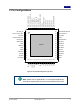
Jennic A.4 Device Package Marking The diagram below shows the package markings for JN5139 devices. The package on the left along with the legend information below it, shows the general format of package marking. The package on the right shows the specific markings for a JN5139-Z01 device, that came from assembly build number 1000004 and was manufactured week 4 of 2007.
Jennic A.5 Tape and Reel Information A.5.1 Tape Orientation and Dimensions The general orientation of the 56QFN package in the tape is as shown in Figure 42. Figure 44: Tape and Reel orientation Figure 43 shows the detailed dimensions of the tape used for 8x8mm 56QFN devices. Reference Ao Bo Ko P T W Dimensions (mm) 8.30 ±0.10 8.30 ±0.10 1.10 ±0.10 12.00 ±0.10 0.30 ±0.10 16.00 +0.30/-0.10 Figure 45: Tape Dimensions © Jennic 2008 JN-DS-JN5139 v1.
Jennic A.5.2 Reel Information: 7” Reel 9 11 Surface Resistivity Between 10e – 10e Ohms Square Material High Impact Polystyrene, environmentally friendly, recyclable All dimensions and tolerances are fully compliant with EIA-481-B and are specified in millimetres. 6 window design with one window on each side blanked to allow adequate labelling space. Tape Width A B (min) C N W (min) W (max) 16 180 1.5min 13 ±0.2 60 +0.1 –0.0 16.40 17.90 Figure 46: Reel Dimensions 68 JN-DS-JN5139 v1.
Jennic A.5.3 Reel Information: 13” Reel 9 11 Surface Resistivity Between 10e – 10e Ohms Square Material High Impact Polystyrene with Antistatic Additive All dimensions and tolerances are fully compliant with EIA-481-B and are specified in millimetres. 3 window design to allow adequate labelling space. Tape Width A B (min) C D (min) N (min) W (min) W (max) 16 330 1.5 13 +0.5 -0.2 20.2 100 15.90 19.40 Figure 47: Reel Dimensions A.5.
Jennic A.6 PCB Design and Reflow Profile PCB and land pattern designs are key to board level reliability, and Jennic strongly recommends that users follow the design rules listed in IPC-SM-782. For reflow profiles, it is recommended to follow the reflow profile in Figure 48 as a guide, as well as the paste manufacturers guidelines on peak flow temperature, soak times, time above liquidus and ramp rates. Figure 48: Reflow Profile 70 JN-DS-JN5139 v1.
Jennic Appendix B Development Support B.1 Crystal Oscillator 16MHz Crystal Requirements Parameter Min Typ Crystal Frequency Max 16MHz Crystal Tolerance Crystal ESR (Rm) Notes 40ppm 1 20Ω 60Ω Crystal Load Capacitance (CL) 9pF External Capacitors (C1 & C2) 15pF Including temperature and ageing See below for more details See below for more details Total external capacitance needs to be 2*CL. , allowing for stray capacitance from chip, package and PCB B.1.
Jennic B.1.2 Crystal Load Capacitance The crystal load capacitance is the total capacitance seen at the crystal pins, from all sources. As the load capacitance (CL) affects the oscillation frequency by a process known as ‘pulling’, crystal manufacturers specify the frequency for a given load capacitance only. A typical pulling coefficient is 15ppm/pF, to put this into context the maximum frequency error in the IEEE802.15.4 specification is +/-40ppm for the transmitted signal.
Jennic This can be used to give an equation for the required transconductance. gm ≥ 4 Rm×ω 2[CS (CT 1+CT 2)+CT 1×CT 2]2 CT 1×CT 2 Example: Using typical parameters of Rm =40Ω, CS =1pF and CT 1 = CT 2 =18pF ( for a load capacitance of 9pF), the equation above gives the required transconductance ( gm ) as 647uA/V. The JN5139 has a typical value for transconductance of 1.25mA/V The example and equation illustrate the trade-off that exists between the load capacitance and crystal ESR.
Jennic B.2 16MHz Oscillator The JN5139 contains the necessary on-chip components to build a 16 MHz reference oscillator with the addition of an external crystal resonator and two tuning capacitors. The schematic of these components are shown in Figure 49. The two capacitors, C1 and C2, should be 15pF ±5% and use a COG dielectric. For a detailed specification of the crystal required see Appendix B.1.
Jennic B.3 Applications Information B.3.
Jennic B.3.2 PCB Requirements Jennic recommend that a standard 4–layer printed circuit board be used for design, with the individual layers organised as shown below in . Copper (0.5 oz – 17 µm) Dielectric FR4 pre-preg 0.009” x 1 A Copper (0.5 oz – 17 µm) B Dielectric FR4 0.02” x 1 Copper (0.5 oz – 17 µm) A Dielectric FR4 pre-preg 0.009” x 1 Copper (0.5 oz – 17 µm) Top Metal Dielectric 1 Mid 1 metal Dielectric 2 Mid 2 metal Dielectric 3 Bottom metal Total Dimension (mm) 0.017 0.2286 0.017 0.508 0.
Jennic B.3.3 Supply Decoupling C12 is the decoupling capacitor for the analogue areas of IC1. It is placed as close as possible to the IC1 pin VDD1. C13 is the decoupling capacitor for the digital areas of IC1. It is also used to decouple the supply on the Flash memory due to: • placement of the Flash memory power pin (IC2 Pin 8) next to the IC1 Pin VDD2 • the fact that the Flash memory is only used during booting (unless reprogramming), so the RF areas of the device are not active. B.3.
Jennic B.3.7 VCO Tune Circuit Layout Considerations The layout of these components is such that all three components are close together, and close to the VCO_TUNE and VB_VCO pins on the wireless microcontroller IC. This improves the performance of the PLL by reducing parasitic impedance and the likelihood of cross-talk. B.3.8 Radio Front-End The radio part of the wireless microcontroller device has an internal transmit-receive switch connected to the external pins on the chip (RF- and RF+).
Jennic • The second layer is Ground and has no tracks on it. This allows the best return path for all RF signals and will reduce noise effects. • The bottom layer contains all other signals and the Vcc power supply for the module. • The ground planes on all layers stop BEFORE the antenna, so that the performance of the antenna is not affected. The recommended antenna clearance for a surface-mounted ceramic antenna is shown below.
Jennic Figure 54: Recommended Solder Paste Mask for 56QFN Package • Nine vias are applied to the paddle. These allow excess solder paste and heated air to be vented away from the device, preventing the device from being lifted during soldering. Figure 55: Vias on the Paddle of the 56QFN Package B.3.12 Bespoke Solutions - PCB Layout Suggestions The list presented below provides some key suggestions when using a wireless microcontroller on a bespoke, multilayer PCB.
Jennic • VCOTune circuit: The components defined in the schematic should be used in order to set the PLL bandwidth correctly. It is also essential to keep these components close to the chip, with minimum track lengths. B.3.13 Using a Balun When using a single ended antenna, the wireless microcontroller will use a balun and should be connected as indicated in Figure 56. The tracks between IC1 pins RF+ and RF-, and the balanced side of the balun, are on the top layer.
Jennic B.3.15 Internal Regulator Smoothing Capacitors A ceramic 100-nF capacitor should be connected to each of the following pins. Place these capacitors close to the device and make the tracks as thick as possible to improve RF bypass/decoupling. Some pins require an additional 47-pF capacitor. Details are given below. Pin Name 47-pF Capacitor Required VB_DIG1 VB_SYN VB_VCO VB_RF VB_A VB_DIG2 VB_MEM B.3.16 VREF A ceramic 100-nF capacitor should be placed as close as possible to the VREF pin.
Jennic Appendix C Related Documents [1] IEEE Std 802.15.4-2003 IEEE Standard for Information technology – Part 15.
Jennic Disclaimers The contents of this document are subject to change without notice. Jennic reserves the right to make changes, without notice, in the products, including circuits and/or software, described or contained herein in order to improve design and/or performance. Information contained in this document regarding device applications and the like is intended through suggestion only and may be superseded by updates.
Jennic Contact Details Corporate Headquarters Jennic Ltd, Furnival Street Sheffield S1 4QT, UK Tel: +44 (0)114 281 2655 Fax: +44 (0) 114 281 2951 info@jennic.com www.jennic.com Jennic Ltd Japan Osakaya building 4F 1-11-8 Higashigotanda Shinagawa-ku Tokyo 141-0022, Japan Tel: +81 3 5449 7501 Fax: +81 3 5449 0741 info@jp.jennic.com www.jennic.com Jennic Ltd Taiwan 19F-1, 182, Sec.2 Tun Hwa S. Road. Taipei 106, Taiwan Tel: +886 2 2735 7357 Fax: +886 2 2739 5687 info@tw.jennic.com www.jennic.