
User's Manual


Jennic
JennicJennic
Jennic
8 JN-DS-JN5148-001-Myy 1v1 © Jennic 2009
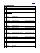
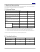
Pin
Signal Function Alternative Function
31 DIO15/SIF_D Serial Interface data / Intelligent Peripheral data
output
General Purpose Digital I/O DIO15
32 DIO16 Intelligent Peripheral data in General Purpose Digital I/O
33 DIO17CTS1
UART1 Clear To Send (input)/ Intelligent
Peripheral device select
General Purpose Digital I/O DIO17
34 DIO18/RTS1 UART1 Request To Send (output)/ Intelligent
Peripheral Interrupt
General Purpose Digital I/O DIO18
35 DIO19/TXD1 UART1 Transmit Data (output) General Purpose Digital I/O DIO19
36 DIO20/RXD1 UART1 Receive Data (input) General Purpose Digital I/O DIO20
37 COMP1-
38 COMP1+
Comparator 1 inputs
39 ADC1 Analogue to Digital input
40 ADC2 Analogue to Digital input
41 ADC3 Analogue to Digital input
*: These two pins are not connected for High power modules
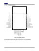
4.2. Pin Descriptions
All pins behave as described in the JN-DS- JN5148 Wireless Microcontroller Datasheet [2], with the exception of the
following:
4.2.1 Power Supplies
A single power supply pin, VDD is provided. Separate analogue (VSSA) and digital (GND) grounds are provided.
These should be connected together at the module pins.
4.2.2 SPI Memory Connections
SPISWP is a write protect pin for the serial flash memory. This should be held low to inhibit writes to the flash device.
SPISSZ is connected to SPI Slave Select 0 on the JN5148.
SPISSM is connected to the Slave Select pin on the memory.
This configuration allows the flash memory device to be programmed using an external SPI programmer if required.
For programming in this mode, the JN5148 should be held in reset by taking RESETN low. Two potential flash 4MB
memory devices may be used in the module, the Numonyx M25P40 and the SST SST25VF040B.
The memory can also be programmed over the UART by using the flash programmer software provided by Jennic.
This is available as part of the Software Developer kit and libraries available from Jennic’s support website –
www.jennic.com/support. To enter this programming mode, SPIMISO (pin 7) should be held low whilst the chip is
reset. Once programming has finished, the chip should be reset, when it will execute the new code downloaded.
For normal operation of the module and programming over the UART, SPISSZ should be connected to
SPISSM.