
User Manual


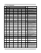


Table Of Contents

4 JN-DS-JN5148-001-Myy 1v5 © NXP Laboratories UK 2012
2. Specifications
Most specification parameters for the modules are specified in the chip datasheet - JN-DS-JN5148 Wireless
Microcontroller Datasheet, [2]. Where there are differences, the parameters are defined here.
VDD=3.0V @ +25°C
Typical DC Characteristics
Notes
JN5148-001-
M00/03
JN5148-001-
M06
Deep sleep current
1.3uA
120nA
Sleep current
2.6uA
1.25uA
With active sleep timer
Radio transmit current (M04 Compatibility Mode)
15mA
84mA
CPU in doze, radio transmitting
Radio transmit current
-
178mA
CPU in doze, radio transmitting
Radio transmit current (ETSI Mode)
-
48mA
CPU in doze, radio transmitting
Radio receive current
17.5mA
23mA
CPU in doze, radio receiving
Centre frequency accuracy +/-25ppm +/-25ppm
Additional +/-15ppm allowance for
temperature and ageing
Typical RF Characteristics
Notes
Receive sensitivity -95dBm -100dBm
Nominal for 1% PER, as per
802.15.4 section 6.5.3.3 (Note 1)
Transmit power (M04 Compatibility Mode)
+2.5dBm
+18dBm
Nominal (Note 2)
Transmit power
-
+22dBm
Nominal
Transmit power (ETSI Mode)
-
+8dBm/MHz
Nominal (Note 3)
Maximum input signal +5dBm -5dBm
For 1% PER, measured as
sensitivity
RSSI range
-95 to -10
dBm
-105 to -20
dBm
RF Port impedance – uFl connector
50 ohm
50 ohm
2.4 - 2.5GHz
Rx Spurious Emissions
-61dBm
-69dBm
Measured conducted into 50ohms
Tx Spurious Emissions
-40dBm
-49dBm
Measured conducted into 50ohms
VSWR (max)
2:1
2:1
2.4 - 2.5GHz
Peripherals
Notes
Master SPI port
5 selects
3 selects
250kHz - 16MHz
Slave SPI port
250kHz - 8MHz
Two UARTs
16550 compatible
Two-wire serial I/F (compatible with SMbus & I
2
C)
Up to 400kHz
Three programmable Timer/Counters with
capture/compare facility, Tick timer
16MHz clock
Two programmable Sleep Timers
32kHz clock
Digital IO lines (multiplexed with UARTs, timers
and SPI selects)
21
19
Four channel Analogue-to-Digital converter
12-bit, up to 100ks/s
Two channel Digital-to-Analogue converter
12-bit, up to 100ks/s