
User Manual

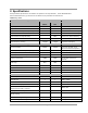

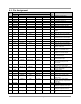


Table Of Contents

© NXP Laboratories UK 2012 JN-DS-JN5148-001-Myy 1v5 9
33 DIO17 CTS1 IP_SEL DAI_SCK JTAG_TCK CMOS
DIO17, UART 1 Clear To Send
Input, Intelligent Peripheral Device
Select Input or Digital Audio Clock
or JTAG CLK
34 DIO18 RTS1 IP_INT DAI_SDOUT JTAG_TMS CMOS
DIO18, UART 1 Request To Send
Output, Intelligent Peripheral
Interrupt Output or Digital Audio
Data Output or JTAG Mode Select
35 DIO19 TXD1 JTAG_TDO CMOS
DIO19 or UART 1 Transmit Data
Output or JTAG Data Out
36 DIO 20 RXD1 JTAG_TDI CMOS
DIO 20, UART 1 Receive Data
Input or JTAG data In
37 COMP1- 3.3V Comparator 1 Input -ve
38 COMP1+ 3.3V Comparator 1 Input +ve
39 ADC1 3.3V Analogue to Digital Input
40 ADC2 3.3V Analogue to Digital Input
41 ADC3 3.3V Analogue to Digital Input
42
VREF
3.3V
Analogue Peripheral Reference
Voltage
43 NC
+
Do Not Connect
*: These two pins are not connected for High power modules
: These two pins are only used on the High power modules
4.2. Pin Descriptions
All pins behave as described in the JN-DS-JN5148 Wireless Microcontroller Datasheet [2], with the exception of the
following:
4.2.1 Power Supplies
A single power supply pin, VDD is provided. Separate analogue (VSSA) and digital (GND) grounds are provided.
These should be connected together at the module pins.
4.2.2 SPI Memory Connections
SPISWP is a write protect pin for the serial flash memory. This should be held low to inhibit writes to the flash device.
SPISSZ is connected to SPI Slave Select 0 on the JN5148.
SPISSM is connected to the Slave Select pin on the memory.
This configuration allows the flash memory device to be programmed using an external SPI programmer if required.
For programming in this mode, the JN5148 should be held in reset by taking RESETN low. Two potential flash 4Mbit
memory devices may be used in the module, the Micron M25P40 and the Winbond W25X40BLSN.
The memory can also be programmed over the UART by using the flash programmer software provided by NXP. This
is available as part of the Software Developer kit and libraries available from www.nxp.com/jennic. To enter this
programming mode, SPIMISO (pin 7) should be held low whilst the chip is reset. Once programming has finished, the
chip should be reset, when it will execute the new code downloaded.
For normal operation of the module and programming over the UART, SPISSZ should be connected to
SPISSM.