
User's Guide


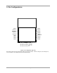


Table Of Contents
- 1. Introduction
- 2. Specifications
- 3. Pin Configurations
- 4. Electrical Characteristics
- Appendix A Additional Information
- A.1 Outline Drawing
- A.2 Module PCB Footprint
- A.3 Optimal PCB placement of the JN5168-001-M00 Module
- A.4 JN5168-001-M00 Antenna Radiation Pattern
- A.5 Manufacturing
- A.5.1 Reflow Profile
- A.5.2 Soldering Paste and Cleaning
- A.6 Ordering Information
- A.7 Related Documents
- A.8 Federal Communication Commission Interference Statement
- A.8.1 Antennas approved by FCC for use with JN5168 modules
- A.8.2 High Power Module usage limitation
- A.8.3 FCC End Product Labelling
- A.9 Industry Canada Statement
- A.9.1 Industry Canada End Product Labelling
- A.10 European R & TTE Directive 1999/5/EC Statement
- A.11 RoHS Compliance
- A.12 Status Information
- A.13 Disclaimers
- Version Control

6 JN-DS-JN5168-001-Myy 1v0 © NXP Laboratories UK 2012
3. Pin Configurations
10
ADC1
SPICLK
SPIMISO
SPIMISI
SPISSZ
DIO0
DIO1
DIO2
DIO3
DIO4
DIO5
DIO6
DIO7
DIO8
DIO9
DIO10
VDD
GND
ADC2
DIO17
DIO16
DIO15
DIO14
DIO13
RESETN
DIO12
DIO11
1
2
3
4
5
6
7
8
9
11 12 13 14 15 16 17 18
27
26
25
24
23
22
21
20
19
Figure 1: Pin Configuration (top view)
Note that the same basic pin configuration applies for all module designs. However, DIO3 (pin 9) and DIO2 (pin 8)
are not available on the JN5168-001-M05 and JN5168-001-M06.