
Datasheet


74ABT16244A All information provided in this document is subject to legal disclaimers. © NXP B.V. 2011. All rights reserved.
Product data sheet Rev. 8 — 3 November 2011 5 of 15
NXP Semiconductors
74ABT16244A
16-bit buffer/line driver; 3-state
6. Functional description
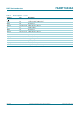
[1] H = HIGH voltage level;
L = LOW voltage level;
X = don t care;
Z = high-impedance OFF-state.
7. Limiting values
[1] The input and output voltage ratings may be exceeded if the input and output current ratings are observed.
[2] The performance capability of a high-performance integrated circuit in conjunction with its thermal environment can create junction
temperatures which are detrimental to reliability.
8. Recommended operating conditions
Table 3. Function table
[1]
Control Input Output
nOE nAn nYn
LLL
HH
HXZ
Table 4. Limiting values
In accordance with the Absolute Maximum Rating System (IEC 60134).
Symbol Parameter Conditions Min Max Unit
V
CC
supply voltage 0.5 +7.0 V
V
I
input voltage
[1]
1.2 +7.0 V
V
O
output voltage output in OFF-state or HIGH-state
[1]
0.5 +5.5 V
I
IK
input clamping current V
I
< 0 V 18 - mA
I
OK
output clamping current V
O
< 0 V 50 - mA
I
O
output current output in LOW-state - 128 mA
output in HIGH-state - 64 mA
T
j
junction temperature
[2]
- 150 C
T
stg
storage temperature 65 +150 C
Table 5. Operating conditions
Voltages are referenced to GND (ground = 0 V).
Symbol Parameter Conditions Min Typ Max Unit
V
CC
supply voltage 4.5 - 5.5 V
V
I
input voltage 0 - V
CC
V
V
IH
HIGH-level input voltage 2.0 - - V
V
IL
LOW-level Input voltage - - 0.8 V
I
OH
HIGH-level output current 32 - - mA
I
OL
LOW-level output current - - 64 mA
t/V input transition rise and fall rate - - 10 ns/V
T
amb
ambient temperature in free air 40 - +85 C