
Datasheet


Philips Semiconductors Product specification
74ABT244Octal buffer/line driver (3-State)
1998 Jan 16
3
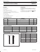
LOGIC SYMBOL
1OE
1
1A0
2
1A1
4
1A2
6
1A3
8
2OE
19
2A3
11
2A2
18
13
2A1
15
16
2A0
17
14
12
1Y0
1Y1
1Y2
1Y3
2Y3
2Y2
2Y1
2Y0
9
7
5
3
SA00149
LOGIC SYMBOL (IEEE/IEC)
1
2
18
4
16
6
14
8
12
19
11 9
13 7
15 5
17
3
EN
EN
SA00150
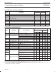
FUNCTION TABLE
INPUTS OUTPUTS
1OE 1An 2OE 2An 1Yn 2Yn
L L L L L L
L H L H H H
H X H X Z Z
H = High voltage level
L = Low voltage level
X = Don’t care
Z = High impedance “off” state
ABSOLUTE MAXIMUM RATINGS
1,
2
SYMBOL
PARAMETER CONDITIONS RATING UNIT
V
CC
DC supply voltage –0.5 to +7.0 V
I
IK
DC input diode current V
I
< 0 –18 mA
V
I
DC input voltage
3
–1.2 to +7.0 V
I
OK
DC output diode current V
O
< 0 –50 mA
V
OUT
DC output voltage
3
output in Off or High state –0.5 to +5.5 V
I
OUT
DC output current output in Low state 128 mA
T
stg
Storage temperature range –65 to 150 °C
NOTES:
1. Stresses beyond those listed may cause permanent damage to the device. These are stress ratings only and functional operation of the
device at these or any other conditions beyond those indicated under “recommended operating conditions” is not implied. Exposure to
absolute-maximum-rated conditions for extended periods may affect device reliability.
2. The performance capability of a high-performance integrated circuit in conjunction with its thermal environment can create junction
temperatures which are detrimental to reliability. The maximum junction temperature of this integrated circuit should not exceed 150°C.
3. The input and output voltage ratings may be exceeded if the input and output current ratings are observed.